http://dx.doi.org/10.7840/kics.2015.40.7.1347
시분할 센싱 기법 기반의 출력 안정화를 위한 10 Gb/s 4채널 VCSELs 드라이버의 구현
양 충 열, 이 강 윤*, 이 상 수°, 정 환 석*
Implementation of 10 Gb/s 4-Channel VCSELs Driver Chip for Output Stabilization Based on Time Division Sensing Method
Choong-reol Yang, Kang-yoon Kee*, Sang-soo Lee°, Whan-seok Jung*
요 약
0.13-μm CMOS 공정기술을 이용하여 10 Gb/s 4채널 수직공진 표면 광레이저 (VCSEL) 드라이버 어레이를 구 현하였다. 높은 전류 해상도, 전력 소모 및 칩 면적의 향상을 위해 시분할 센싱기법을 사용한 디지털 APC/AMC 가 최초로 채택되었다. 측정된 –3 dB 주파수 대역폭은 9.2 GHz이고, 소신호 이득은 10.5 dB, 그리고 전류 해상 도는 폭넓은 온도 범위에 대해 10 Gb/s 까지 안정한 파장동작을 위한 1 mA/step이다. 제안된 APC/AMC는 5 ~ 20 mA 의 바이어스 전류 제어 및 5 ~ 20 mA 의 변조전류제어를 입증하였다. 4 채널 칩 소모전력은 최대 바이 어스 및 변조전류 하에서 371 mW, 칩 사이즈는 3.71 x 1.3 mm2이다.
Key Words : TWDM-PON, VCSEL Driver, Time Division sensing method, CMOS, APC ABSTRACT
We implemented a 10 Gb/s 4-channel vertical cavity surface emission lasers (VCSEL) driver array in a 0.13 μ m CMOS process technology. To enhance high current resolution, power dissipation, and chip space area, digital APC/AMC with time division sensing technology is primarily adopted. The measured -3 dB frequency bandwidth is 9.2 GHz; the small signal gain is 10.5 dB; the current resolution is 0.01 mA/step, suitable for the wavelength operation up to 10 Gb/s over a wide temperature range. The proposed APC and AMC demonstrate 5 to 20 mA of bias current control and 5 to 20 mA of modulation current control. The whole chip consumes 371 mW of low power under the maximum modulation and bias currents. The active chip size is 3.71 x 1.3 mm
2.
First Author : ETRI Optical Internet Dept. [email protected], regular member
° Corresponding Author : SungKyunKwan University Electro-Electric Engineering dept. [email protected], regular member
* ETRI Optical Internet Dept. [email protected], [email protected], 정회원
논문번호:KICS2015-02-038, Received February 16, 2015; Revised June 29, 2015; Accepted June 29, 2015
Ⅰ. 서 론
The sudden high increase in demand for high-speed access networks has led to the recognition of low-cost optical access systems as the most viable technology available. Recently, the time
division multiplexing- passive optical network stage 2 (TWDM-PON)[1] architecture with centralized VCSEL at the optical line terminal (OLT) has emerged as an attractive solution for low-cost implementation. The next generation passive optical network stage 2 (TWDM-PON) utilizes WDM and
TDM methods to assign a private wavelength between the OLT and optical network unit (ONU) in order to support TWDM-PON through a time division system.
Most optical transmitters are required to maintain system performance stability, such as average optical power and extinction ratio over a wide temperature range (-40℃ to 80℃). In order to obtain reliable and constant transmitted optical power over this wide temperature, the characteristics of VCSEL should be confirmed according to temperature variation through a VCSEL driver. The trend recent high-speed VCSEL drivers has shifted to using highly productive and integrated CMOS technology[2].
To provide stable driving, fast settling time and high resolution of VCSEL, the AC compensates for the actual power level by controlling common mode (CM) value of VCSEL driver. The AMC minimizes errors of process, voltage, and temperature, as well as influences of aging based on usages by controlling output amplitude of the drive system to be constant so that it minimizes data error to be transferred with a constant power. The existing CMOS process based on a high speed VCSEL driver was proposed in an analogue type that requires a dummy VCSEL device or MPD that operates in the same way with VCSEL device that sends light signals or that requires more trans-impedance amplifiers (TIA)[3] to realize APC/AMC. Moreover, the dummy VCSEL device, MPD, and TIA amplifier are all components of circuits that are attached to an external VCSEL driver, which introduced uneconomical problems with more complications and expanding volumes.
Thus, there was a growing need for a VCSEL driver that can realize APC/AMC functions at a lower cost based on CMOS processes which did not require these additional circuit factors.
There are two ways to realize the existing APC/AMC. One is to apply one ADC to each channel; the other is to apply it commonly to multi-channels from one APC/AMC. For the former, the number of required ADC increases according to the number of ADC, while the current sinking and
the area increases as the number of bit of ADC increases to realize high resolution APC/AMC. On the other hand, the latter can decrease the area, while current sinking increases sharply as controller for APC/AMC attempts to be realized for each channel to compensate disadvantages of lower precision, as each channel has a different output power source with no guarantees for power and modulation of each channel. This paper suggests APC and AMC methods through a digital loop using a time sharing sensing method. Here, the optical TDM (OTDM) system[4] concept is applied to the inner circuit of the transmitter (VCSEL) driver, so that 4 channel VCSEL driver sensing[5] is performed by using time sharing concept, applying the APC/AMC of the digital method to each 4 channels for automatic calibration of the power. Since this proposed sensing method can be applied to every channel with one sensing block, it provides a cost-effective resolution for multi-channel application by low power consumption[6] and chip miniaturization because the circuit size and current consumption are reduced to be 1/n based on the number of times the block is shared and used.
Ultimately, this proposal is a brand new method that has not been applied to multi-channel a VCSEL driver design up till now. This proposal could bring about considerable cost reduction when applied to an optical communication system. In this paper, the design and implementation of 10 Gb/s x 4 channel CMOS VCSEL driver array for TWDM applications is reported.
Ⅱ. Proposed VCSEL Driver
Figure 1 shows the block diagram of a main driver with auto optical power control. The main driver is to provide sufficient current for the VCSEL. IBIAS represents the bias current of the VCSEL corresponding to the nominal threshold current, whereas the modulation current (IMOD) represents the modulation current of the VCSEL corresponding to the optical output swing range; it guarantees the VCSEL operation. IBIAS always flows through VCSEL to guarantee IBIAS (bias
그림 2. AMC/APC 피드백을 갖는 메인드라이버 코어 회로.
Fig. 2. Schematic of Main driver core with APC/AMC feedback loop.
그림 3. CM 검출기 및 피크 검출기.
Fig. 3. CM Detector and Peak Detector.
그림 1. 제안된 시분할 센싱기술의 VCSEL 드라이버.
Fig. 1. Proposed VCSEL driver with time division sensing Techniques.
current) exceeds threshold current. IMOD flows through VCSEL according to the incident voltage signal. To compensate for the temperature effect, because the characteristics of VCSEL change with time and temperature, APC and AMC are essentially required. To implement the auto control method, we needed to detect optical power. We exploited a new APC/AMC feedback loop[7] instead of the existing MPD method[8] for the detection of optical power.
The proposed VCSEL Driver configuration with Time Division Sensing Technique for TWDM Applications is presented in Figure 1.
Figure 2 could reduce the current sinking and area for the same conversion speed to be at 1/2 level by using time shared ADC for each channel of Driver 2, while not using one ADC for each channel for APC/AMC. The output CM voltage of the VCSEL driver acquired from the CM sensing circuit inside the Peak Detector of Driver 1~4 and the amplitude value sensed from the amplitude sensing circuit are selected through the MUX of the second level, where the selecting signal is created through the APC/AMC controller.
Figure 3 shows the blocks of the CM Detector and the Peak Detector. The CM Detector senses the output CM level of the VCSSEL driver, while the Peak Detector senses the amplitude of output.
Ripples created from the process of sensing voltage levels are reduced through a low pass filter (LPF), then through band gap adaption (BGA) and amplified according to 10 bit ADC input range. The CM Detector and Amplitude Detector are transferred to 10 bit ADC through the Mux. The time
transferred to the Multiplexer is set from the AMC/APC controller as it senses stable voltage within a sufficient amount of time.
Figure 4 shows the APC/AMC function using the time sharing sensing method[4]. It is designed in a way to automatically compensate for power as a result of realizing automatic APC/AMC by printing the Bit<9:0> that controls the APC/AMC through the computation of digitalized information after converging the amplitude of voltage into digital through ADC by using a peak detector. A printed DIG_APC<9:0> controls BIAS current, while DIG_AMC<9:0> controls IMOD and IBIAS. Here, the current resolution required by TWDM is increased by using 10 bit ADC. It is possible to increase the precision and reduce current sinking and die size as time sharing sensing is applied to all channels for APC/AMC function. For the higher current resolution required by TWDM, it is designed to be 10 bit ADC, by combining a 4 bit flash and
그림 4. APC/AMC 블록도.
Fig. 4. APC/AMC block diagram.
그림 5. ADC 블록도.
Fig. 5. ADC block diagram.
그림 7. 칩 레이아웃.
Fig. 7. Chip layout.
a 6 bit successive approximation register (SAR) ADC.
It is much more advantageous in the aspect of design area and consumed power, compared to the existing technology that uses 10 bit ADC for each channel, as it uses 10 bit ADC after time sharing in the process of calibration via SAR ADC. Here, the time sharing APC/AMC controller is composed of digital logic. APC secures the actual power level by controlling the CM value of the VCSEL driver, while AMC minimizes data errors while transmitting data with constant power by controlling the output amplitude of the driver.
Figure 5 shows the structure of 10 bit Time Interleaved flash SAR ADC. The ADC input circuit receives the output of the Peak Detector and goes through sample and hold procedures. Input sampled through the input circuit goes through two stages of coarse flash ADC and fine SAR ADC via ADC core circuit to create each output. Here, Fine SAR ADC operates in a time interleaved way, so that it gets a higher sampling speed. ADC output circuit then creates the final output bit of ADC by combining
digital bits that are each created from coarse flash ADC and Fine SAR ADC.
Figure 6 shows automatic temperature control (ATC) configuration. ATC is used to ensure the eye diagram opening during the variance of absolute temperature. The operation scheme is shown in Fig.
6. The function of proportional to absolute temperature is to generate the temperature dependent bias voltage which can compensate for the reduction of output power emission of VCSEL as the temperature increases.
그림 6. ATC블록도.
Fig. 6. ATC block diagram.
Ⅲ. Results
The VCSEL driver has been fabricated in a full 0.13-μm CMOS technology. The VCSEL driver operates in the 10 Gb/s at a 3.3 Vdc supply. The chip layout of the 4 channel VCSEL driver array is shown in Figure 7. The channel pitch is 250 μm.
The chip size is 3.1 mm x 1.37 mm.
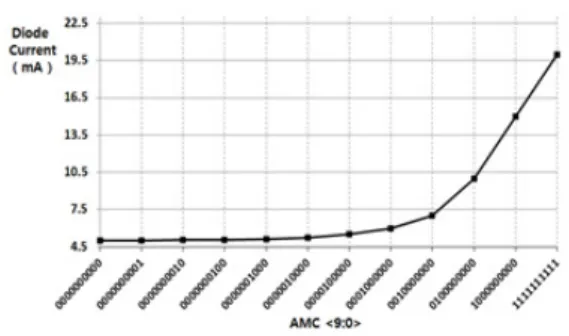
Figure 8 shows Current Resolution & CM Resolution results. The measurement was performed by increasing high rank bit one by one, not by overall measurement for 1,024 bits. This method confirmed the result that each bit has certain steps in an exponential function graph. Current ranges were 5 to 20 mA, while resolution was (20-5)
(a) Current Resolution (CM range : 2.45~3.02V, Resolution : 0.56 mV Current range : 5 ~ 20 mA, Resolution : 0.015 mA).
(b) CM Resolution (CM range : 2.61~3.02 V, Resolution : 0.4 mV Current range : 6 ~ 17 mA, Resolution : 0.011 mA).
그림 8. APC/AMC에서 전류 해상도 및 CM 해상도 결과.
Fig. 8. Current resolution & CM Resolution result at APC and AMC.
(a) The ATC variation of VCSEL driver as temperature changes.
(b) Eye diagram with jitter 6.9271 ps at ATC ON 25℃.
(c) Eye diagram with jitter 3.571 ps at ATC ON 85 ℃.
그림 9. ATC ON ((a) 25℃, (b) 85℃)에서 아이 다이어그 램과 온도가 변할 때 VCSEL 드라이버의 ATC변화.
Fig. 9. The ATC variation of VCSEL driver as temperature changes and Eye diagram at ATC ON ((a) 2 5℃, (b) 85℃)
mA/210 = 0.015 mA/step. Voltage ranges were 2.45 to 3.02 mV, while resolution was 0.56 mV.
Figure 9 is the measurement result of ATC. It confirms the temperature compensation function (a) at -40 to 85 ℃, with ATC function at the centre of APC/AMC. The graph shows the result of swing as a change of diode current based on ATC temperature at the centre of APC/AMC; voltage swing at 85 ℃ was measured to be 316.8 mV.
Based on the measurement results, the temperature compensation progress is shown in the graph based on ATC measurement in -40 to 85 ℃. This shows the Eye Diagram in (b) 25 ℃ and (c) 85 ℃ when ATC/AMC is on. As turn on and off time of the VCSEL diode is fast, so it shows that turn on time at room temperature and 85 ℃ has almost same eye within swing difference of 102 ps.
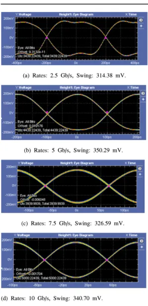
The eye patterns with respect to the data rates from 2.5 Gb/s to 10 Gb/s are measured in Figure 10.
The performance of the proposed VCSEL driver to be used in TWDM-PON is summarized in Table 2.
In TWDM-PON system, a wavelength light source should be initialized for physical layer connection between TX and RX. As changes occur in the peak wavelength of transmitter VCSEL when the surrounding temperature rises in the communication system, it is necessary to have the VCSEL driver in optical module in TWDM-PON system which uses 32 channels.
Use wavelength of NG-PON (TWDM) is in the range of 1576.20 nm to 1582.02 nm, in which 32 channels are allocated in every 0.18 nm.
In case of Raycan 10 Gb/s VCSEL, as the
(a) Rates: 2.5 Gb/s, Swing: 314.38 mV.
(b) Rates: 5 Gb/s, Swing: 350.29 mV.
(c) Rates: 7.5 Gb/s, Swing: 326.59 mV.
(d) Rates: 10 Gb/s, Swing: 340.70 mV.
그림 10. 데이터 아이패턴
Fig. 10. Eye pattern with respect to the data.
channel distance is 0.6 nm, it is necessary to have a VCSEL driver that increases the VCSEL peak wavelength by 0.06 nm when the temperature rises for 1℃. This makes it effective to secure economic feasibility for the development of a low-cost transceiver that has the advantages of low power and miniaturization.
At the end, the required qualification of 10 Gb/s VCSEL driver is 0.06 mA/step and the measured result of current range is 5 to 20 mA. These results show that it is possible for TWDM application with (20-5) mA / 1023 = around 0.02 mA/step].
Ⅳ. Conclusion
A 4 channel CMOS VCSEL driver array is implemented in 0.13 μm CMOS technology. The Optical transmitter drives the VCSEL array, operating at 10 Gb/s with the proposed APC/AMC controller to obtain constant optical output power.
To enhance high current resolution, power dissipation, and chip space area, digital APC/AMC with time division sensing technology is primarily adopted. The time division sensing function is achieved by monitoring the current and eye diagram change of the VCSEL with -40 to 85 ℃ temperature variations. The measured -3 dB frequency bandwidth is 9.2 GHz; the small signal gain is 10.5 dB; the current resolution is 0.01 mA/step, suitable for the wavelength operation up to 10 Gb/s over a wide temperature range. The proposed APC and AMC demonstrate 5 to 20mA of bias current control and 5 to 20 mA of modulation current control. The whole chip consumes 371 mW of low power under the maximum modulation and bias currents. The active chip size is 3.71 x 1.3 mm2.
The driver is suitable for capital expenditures (CAPEX) and operational expenditures (OPEX) high rate optical transceiver when using the CMOS process. Therefore, it can be applied to TWDM for NG-PON. To the knowledge of the authors, it is the first reported time division sensing method based APC/AMC in order to utilize the VCSEL driver array for TWDM applications. The chip can be applied to an optical transceiver in a TWDM PON system as well as optical interconnections between high-speed chips.
References
[1] K. Kim, J. Lee, S. Lee, J. Lee, and Y. Jang,
“Low-cost, Low-power, High capacity 3R OEO-type Reacher Extender for a Long Reach TDMA-PON,” ETRI J., vol. 34, no. 3, pp.
352-359, 2012.
[2] C. Yang and S. Lee, “A High Speed CMOS Arrayed Optical Transmitter for WDM Applications,” J. KICS, vol. 38, no. 6, pp.
427-434, Jun. 2013.
[3] C. Yang, K. Lee, and S. Lee, “A Design and Iimplementation of 4x10 Gb/s Transimpedance Amplifier (TIA) Array for TWDM-PON,” J.
KICS, vol. 39, no. 7, pp. 440-448, Jul. 2014.
[4] Y.-H. Oh, S.-G. Lee, Q. Le, H.-Y. Kang, and T.-W. Woo “A COMS Burst-mode Optical Transmitter for 1.25-Gb/s Ethernet PON Applications,” IEEE Trans. Cir. Syst.-II:
Express Briefs, vol. 52, no. 11, Nov. 2005.
[5] Rodney S. Tuker, G. Eisenstein, and S. K.
Korotky, “Optical Time-Division Multiplexing for Very High Bit-rate Transmission,” J.
Lightwave Technol., vol. 6, no. 11, pp. 1737-
1739, Nov. 1988.[6] G. Sialm, C. Kromer, F. Ellinger, T. Morf, D.
Erni, and H. Jacke, “Design of Lower Power Fast VCSEL Drivers for High-density Links in 90-nm SOI CMOS,” IEEE Trans. Microwave
Theory and Techniques, vol. 54, no. 1, pp. 65
-73, Jan. 2006.[7] S. Galal and B. Razavi, “10-Gb/s Limiting Amplifier and Laser/Modulator Driver in 0.18-um CMOS Technology,” IEEE ISSCC, vol. 1, pp. 188-487, Feb. 2003.
[8] W.-S. Oh, K.-Y. Park, and S. Lee, “A 4-ch 10-Gb/s CMOS VCSEL Driver Array with Adaptive Optical Power Control,” ICACT, vol.
1, pp. 826-829, Phoenix Park, Feb. 2010.
양 충 열
(Choong-reol Yang)1983년 : 건국대학교 전자공학 과 공학사
1998년 : 충남대학교 전자공학 과 공학석사
2007년 : 충남대학교 전자공학 과 공학박사
1992년 6월~현재 : 한국전자통 신연구원 광인터넷연구부 광가입자연구실 책임연 구원
<관심분야> 광통신, 광패킷스위칭, 광인터넷, 아날 로그 집적회로 설계, Ethernet PON
이 강 윤
(Kang-yoon Lee)1996년 : 서울대학교 전기공학 공학사
1998년 : 서울대학교 전기공학과 공학석사
2003년 : 서울대학교 전자공학과 공학박사
2005~2011년 : 건국대학교 전기 전자공학과
2012~2014년 : 성균관대학교 전자전기공학과 부교수
<관심분야> CMOS RF Transceiver, 아날로그 IC, 아날로그-디지털 혼성모드 VLSI 시스템 설계
이 상 수
(Sang-soo Lee)1988년 : 인하대학교 전자공학과 공학사 1990년 : 인하대학교 전자공학과 공학석사 2001년 : 인하대학교 전자공학과 공학박사 1990년 7월 3일~2013년 1월 :한국전자통신연구원 현재 : 광인터넷연구부 광가입자연구실 실장
<관심분야> 광액세스망, WDM-PON
정 환 석
(Hwan-seok Chung)1997년 : 경북대학교 전자공학과 공학사 1999년 : 한국과학기술원 전자공학과 공학석사 2003년 : 한국과학기술원 전자공학과 공학박사 2005년 7월~현재 : 한국전자통신연구원 광인터넷연
구부 광가입자연구실 실장
<관심분야> 광통신망, 광송수신장치, 광액세스망, Ethernet PON