Low cost 2.4-GHz VCO design in 0.18-㎛ Mixed-signal CMOS Process for WSN applications
325
저 가격 0.18-㎛ 혼성신호 CMOS공정에 기반한 WSN용 2.4-GHz 밴드 VCO설계
Low cost 2.4-GHz VCO design in 0.18-㎛
Mixed-signal CMOS Process for WSN applications
Heesauk Jhon
1· Chang-Ho An
2· Youngho Jung
3*1Assistant Professor, Department of Electronics, Information and Communication, Mokpo National University, jeonnam, 58554 Korea
2Assistant Professor, Department of Digital Electronics, Dealim University College, 13916, Korea
3*Assistant Professor, Department of Electronic and Electrical Engineering, Daegu University, Gyeongbuk 38453, Korea
ABSTRACT
This paper demonstrated a voltage-controlled oscillator (VCO) using cost-effective (1-poly 6-metal) mixed signal standard CMOS process. To have the high-quality factor inductor in LC resonator with thin metal thickness, patterned-ground shields (PGS) was adopted under the spiral to effectively reduce the ac current of low resistive Si substrate. And, because of thin top-metal compared with that of RF option (2 μm), we make electrically connect between the top metal (M6) and the next metal (M5) by great number of via array along the metal traces. The circuit operated from 2.48 GHz to 2.62 GHz tuned by accumulation-mode varactor device. And the measured phase noise of LC VCO has –123.7 dBc/Hz at 1MHz offset at 2.62 GHz and the dc-power consumption shows 2.07 mW with 1.8V supply voltage, respectively.
Keywords : Mixed-signal CMOS process, VSI, voltage-controlled oscillator (VCO), phase noise, low cost
Ⅰ. Introduction
With the fast and various developments of battery- operated wireless applications, the requirement for power and cost-effective RFIC has increased, significantly [1]. Especially, wireless sensor networks (WSNs) leads IOT applications combining sensor, dc-power, computation, and RF communication functions into a system. For this case, one of the critical issues is low unit cost compared with other one such as extended lifetimes (power consumption) and circuit performances, since typical sensor network consists of a large number of small and communication module that use point-to-point communication by RF to connect with a self-organized communication network [2].
Based on the discussion, our design focused on small area and using low cost CMOS processes for WSN unit cell. In this paper, the measurement results verified the effectiveness of using digital logic CMOS process (1-poly and 6-metal) in voltage-controlled oscillator (VCO) design with the help of vertical-shunt inductor (VSI).
Ⅱ. LC-VCO Circuit Design methodology for saving the fabrication cost
For LC-VCO design consideration, performance of spiral such as Q-factor in LC tank significantly has effect on the phase-noise and output power, simultaneously. A low cost digital logic CMOS process with thin top metal thickness (< 1.0 um) and vertical-shunt inductor (VSI) are a good candidate for low cost LC VCO [3]. Since, the VSI is designed by connection of two-/or three different kinds of metal layers through via arrays, in our
Received 10 February 2020, Revised 11 February 2020, Accepted 14 February 2020
* Corresponding Author Youngho Jung (E-mail:[email protected], Tel:+82-53-850-6613)
Assistant Professor, Department of Electronic and Electrical Engineering, Daegu University, Gyeongbuk 38453, Korea
Open Access
http://doi.org/10.6109/jkiice.2020.24.2.325
print ISSN: 2234-4772 online ISSN: 2288-4165Short Paper
한국정보통신학회논문지 Vol. 24, No. 2: 325~328, Feb. 2020
한국정보통신학회논문지 Vol. 24, No. 2: 325-328, Feb. 2020
326 design the effective metal thickness of this spiral was increased up to 2.3 μm without any extra cost.
A schematic structure of the LC- VCO is depected in Fig. 1(a). To achieve better phase-noise performance based on waveform symmetry and higher amplitude, two cross-coupled N/PMOS pairs (M1 to M4) were employed;
their positive feedback effectively compensates for the LC-tank loss caused by the VSI and L
2. To adopt the second-harmonic filtering technique in series with the LC-tank, which generally enhance the impedance at 2fo (second harmonic of oscillation frequency), another spiral (L
1) was used.
The LC tank was composed by symmetric/differential VSI of 6 nH and two MOS varactors (V1 and V2). A 6.0-nH VSI has a poly-shielded ground structure and shows the Q-factor of 5 at 2.4 GHz. The accumulation- mode varactor (V1 and V2) with an n+ poly gate in n-well region was to control the range of oscillation frequency. The measured capacitance changes from 230 fF to 290 fF and the Q-factor is greater than 60. The effective parallel conductance of the LC tank was approximately 3.57 mS at 2.4 GHz. From this calculation, the transconductance of NMOS (gmn) and PMOS (gmp) for oscillation should have 10.7 mS at least; Based on that, DC bias current of the VCO is 1.15mA for proper oscillation and low phase noise.
Ⅲ. Experimental VCO TEST-Results
In Fig. 1(b), the Si-area of fabricated VCO (including pads) is 0.9 × 1.0 mm
2. The VSI-based LC-VCO has the following key design parameters: active size M1-M2 (W/L) = 40/0.18 μm, M3-M4 (W/L) = 20/0.18 μm, radius of L
1and L
2= 240 μm and 252μm with values of 6.0 nH at 2.4 GHz. To suppress substrate loss of the spiral, grounded metal-1 shields were applied underneath the MIM-capacitors and the many of RF interconnection lines [3]. Fig.2 shows the measurement results for output signal, phase noise performance with 1MHz offset freqeuncy and tuning range of VCO. An output power greater than –9.9 dBm was achieved with 2.1 mW of DC power consumption. Fig.2 (c) depicted the simulation and measurement results about tuning range that the simulation error has less than 3%. The frequency range shows from 2.48 GHz to 2.62 GHz as a function of the control voltage (Vc) with tuning range of 140MHz.
Additionally, the phase noise of the fabricated VCO was found to be −123.7 dBc/Hz at a 1-MHz offset.
For the performance comparisons with different oscillators, the general figure of merit (FOM) is evaluated as defined by [4]
× log
×
(1)
(a) (b)
Fig. 1 (a) Designed LC VCO schematic diagram (b) Chip microphotograph (0.9 mm × 1.0 mm).
Low cost 2.4-GHz VCO design in 0.18-㎛ Mixed-signal CMOS Process for WSN applications
327 Where L (f
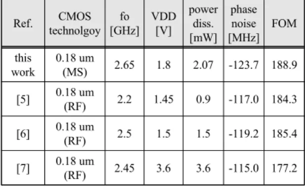
m) means the phase noise at an offset frequency from the fo which means RF carrier frequency of LC VCO . Table. 1 summarizes the other VCO results that were previous reported in [5] –[7] implemented by RF option. We confirms that our design has a comparable FOM with cost-saving advantages.
(a)
(b)
(c)
Fig. 2 (a) Output power of fabricated LC VCO (b) phase noise performance at 1MHz offset frequency (c) tuning range performance compared with simulation results.
Table. 1 Performance comparison of LC VCO
Ref. CMOS
technolgoy fo [GHz]
VDD [V]
power diss.
[mW]
phase noise [MHz]
FOM
this work
0.18 um
(MS) 2.65 1.8 2.07 -123.7 188.9
[5] 0.18 um
(RF) 2.2 1.45 0.9 -117.0 184.3
[6] 0.18 um
(RF) 2.5 1.5 1.5 -119.2 185.4
[7] 0.18 um
(RF) 2.45 3.6 3.6 -115.0 177.2
Ⅳ. Conclusion
In our research, the feasibility of low cost RFIC was demonstrated by fabrication in a 0.18- μ m digital CMOS process. VSI with PGS has compensation of critical demerit of thin metal thickness and low Si-resistivity of logic CMOS process. The proposed LC VCO consumes 2.1 mW dc-power dissipation and achieves a phase noise of −123.7 dBc/Hz at 1-MHz offset at 2.62 GHz frequency.
ACKNOWLEDGEMENT
This work was supported by the National Research Foundation of Korea (NRF) grant funded by the Korea government (MSIT) (2019R1F1A1056151)
REFERENCES
[ 1 ] Y. Yao, Q. Cao, and A. V. Vasilakos, “An energy-efficient, delay-aware, and lifetime-balancing data collection protocol for heterogeneous wireless sensor networks,” IEEE/ACM Trans Net. vol. pp. 810-823, 2015.
[ 2 ] W. Contreas, and S. Ziavras, “Low-Cost, Efficient Output- Only Infrastructure Damage Detection With Wireless Sensor Networks,” IEEE Transactions on Systems, Man, and Cybernetics: Systems. vol. 50. no. 3, pp. 1003-1021, Jul.
2020.
[ 3 ] H. Jhon, H. M.-S . Kim, and M. Kang, “Cost-Effective 4
한국정보통신학회논문지 Vol. 24, No. 2: 325-328, Feb. 2020
328
GHz VCO Using Only Miniature Spirals Realized in a 0.18 μm CMOS Process for Wireless Sensor Network (WSN) Applications,” MDPI Electronics. vol. 11. 1369, 2019.[ 4 ] R. Wu, J. Chen, and X. Fang, “A Novel On-Chip Transformer With Patterned Ground Shield for High Common-Mode Transient Immunity Isolated Signal Transfer,” IEEE Electron Device Letters, vol.11, no. 13, pp. 1712-1715, Nov.
2018.
[ 5 ] D. Park, and S.-Hwan. Cho, “A 1.8 V 900 ㎼ 4.5 GHz VCO and Prescaler in 0.18 ㎛ CMOS Using Charge-Recycling Technique,” IEEE Microw.Wireless Compon. Lett.,, vol. 19, no. 2, pp.104-106, Feb. 2009.
[ 6 ] J. Gil, S.-S. Song, H. Lee, and H.Shin, “A-119.2 dBc/Hz at 1 MHz, 1.5 mW, Fully Integrated, 2.5-GHz, CMOS VCO Using Helical Inductors,” IEEE Microw.Wireless Compon.
Lett., vol. 13, no. 11, pp. 457-459, Nov. 2003.
[ 7 ] D. Leenaerts, C. Dijkmans, and M. Thompson, “A 0.18-㎛
CMOS 2.45 GHz, low-power quadrature VCO with 15%
tuning range,” IEEE MTT-S, pp. 67-70, 2002.