Synthesis of vertically aligned thin multi-walled carbon nanotubes on silicon substrates using catalytic chemical vapor deposition and their field emission
properties
S. I. Jung, S. K. Choi, S. B. Lee*
Department of Nanoscale Semiconductor Engineering, Hanyang University, Seoul 133-791 (Received June 2 2008, Revised July 7 2008, Accepted July 8 2008)
We have succeeded in synthesizing vertically aligned thin multi-walled carbon nanotubes (VA thin-MWCNTs) by a catalytic chemical vapor deposition (CCVD) method onto Fe/Al thin film deposited on a Si wafers using an optimum amount of hydrogen sulfide (H2S) additive. Scanning electron microscope (SEM) images revealed that the as-synthesized CNT arrays were vertically well-oriented perpendicular to the substrate with relatively uniform length. Transmission electron microscope (TEM) observations indicated that the as-grown CNTs were nearly catalyst-free thin-MWCNTs with small outer diameters of less than 10nm.
The average wall number is about 5. We suggested a possible growth mechanism of the VA thin-MWCNT arrays. The VA thin-MWCNTs showed a low turn-on electric field of about 1.1 V/μm at a current density of 0.1 μA/cm2 and a high emission current density about 2.5 mA/cm2 at a bias field of 2.7 V/μm. Moreover, the VA thin-MWCNTs presented better field emission stability without degradation over 20 hours (h) at the emission current density of about 1 mA/cm2.
Keywords: Thin multi-walled carbon nanotubes, catalytic chemical vapor deposition, field emission
Ⅰ. Introduction
Carbon nanotubes (CNTs) have been extensively utilized as one of the best field emitters due to their high aspect ratio, high mechanical strength, high electrical conductivity, and strong C-C covalent bonds in graphene layers constituting the nanotubes [1,2]. Recently, thin multi-walled CNTs (thin-MWCNTs) with smaller tip radius and high structural perfection have attracted much attention and been suggested as good candidates for field
emission applications due to their intermediate structural properties among single-walled CNTs (SWCNTs), double-walled CNTs (DWCNTs) and thick-MWCNTs [3,4]. As thin-MWCNTs are composed of 2-6 coaxial graphene layers and diameters of less than 10 nm, they possess excellent electron field emission properties such as a lower onset electric field and higher emission current density as SWCNTs and DWCNTs due to the large field enhancement fac- tor, and also better emission current stability for long operation time as thick-MWCNTs due to the ex-
istence of several graphene layers.
Until now, the thin-MWCNTs have been synthe- sized by various methods such as arc discharge, laser vaporization, and chemical vapor deposition (CVD) [3-5]. Among these synthesis methods, the CVD technique is suitable for synthesizing vertically aligned CNTs (VA CNTs) because it is possible to con- trol the diameter, length and structure of aligned CNTs through process parameters. It is well known that aligned CNTs which are directly grown on a va- riety of substrates are of great importance for a number of nanoelectronic applications such as field emission display [6] and sensors [7]. Many research groups have synthesized various species of VA CNTs such as SWCNTs [8,9], DWCNTs [10,11], and thick-MWCNTs [6,12-15] with an adequately con- trolled length of several tens of mm and several mm.
However, most of the synthesized MWCNTs generally indicated thick diameters about 20~50 nm. Since the field emission from CNTs is strongly dependent on the aspect ratio of CNTs which is inversely propor- tional to the diameter [16], it is expected that thin-MWCNTs show the better field emission per- formance than that of thick-MWCNTs. Recently, the addition of sulfur was found to be effective in pro- moting the growth and the yield of CNTs, resulting in massive growth of super dense and VA CNT forests [17-23]. Hydrogen sulfide (H2S) gases were applied to our process for growing VA thin-MWCNTs. Although VA thin-MWCNT arrays have been grown by various CVD techniques, their field emission performances have not been reported yet [24-27].
In this paper, we report that the VA thin-MWCNTs with a thin diameter of about 10 nm were successfully synthesized by a CCVD method onto Fe/Al thin films deposited on Si wafers. We found that the addition of hydrogen sulfide (H2S) was effective in increasing the growth rate of the CNTs and inducing the vertical alignment of thin-MWCNTs. The well-aligned thin-MWCNTs showed good field emission properties
and strong emission stability.
Ⅱ. EXPERIMENT
Initially, a 10 nm-thick Al film was deposited onto the n-type Si(100) substrate using thermal evapo- ration, followed by a 1 nm-thick Fe film as the catalyst. Pure Ar (99.9%), H2 (99.9%), C2H2 (99.99%) and H2S (1%,diluted by Ar) gases for the synthesis of CNTs were used in this work. The thin-MWCNT growth was carried out in a quartz tube furnace with a 20 mm inner diameter and a 300 mm-long heating zone. The substrate was placed in the center of the heating zone and then the furnace was heated to a temperature of 800oC under 1000 sccm Ar and 50 sccm H2 at one atmosphere. The CNTs were grown at 800oC with C2H2 (30 sccm) and a diluted H2S (0~80 sccm) flow under a Ar/H2 (1000/50 sccm) flow for 20 min.
The as-grown CNTs were characterized by scan- ning electron microscopy (SEM, Hitachi S-4700), high- resolution transmission electron microscopy (HRTEM, FEI Tecnai F-20), and micro-Raman spectroscopy.
The micro-Raman scattering was carried out at room temperature using Ar+ laser excitation at a wave- length of λex = 514.5 nm (LabRam HR-800). Field electron emission measurements were performed us- ing a planar diode configuration in a vacuum chamber at a pressure of 2×10⁻⁷ Torr. The anode was a stain- less steel disk with a diameter of 5 mm. The gap be- tween the cathode and the anode was 270 μm, and the measured emission area was 0.19625 cm2. The emis- sion current was monitored with a Keithley 6517A electrometer and recorded at 1.0 second (s) intervals by applying a sweep step of 20 V.
Ⅲ. RESULTS AND DISCUSSION
Figures 1(a)-(d) show the typical cross-sectional
Fig. 1. SEM images of as-grown CNTs grown at different H2S flow rate: (a)15, (b)30, (c)50, (d)80sccm, (e) and (f) show the SEM images of CNTs synthesized at H2S flow rate of 80 sccm with high magnification.
SEM morphologies of as-grown CNTs on Fe/Al thin film deposited on Si substrates according to the di- luted H2S flow rate. When less than 15 sccm of the diluted H2S was supplied to the reactor, the CNTs were found lying down on the substrate as shown in Figure 1(a). However, with increasing H2S flow rate, the synthesized CNTs are found well-aligned on the substrate. Figures 1(b), (c), and (d) show the cross-sectional SEM images of the as-grown CNTs with the diluted H2S flow rate of 30,50, and 80 sccm, respectively. After a reaction for 20 min, the length of the synthesized CNTs with the H2S flow rates of 30, 50, and 80 sccm were 45, 27, and 17 μm, re- spectively, as shown in Figures 1(b)-(d). When we increased the flow of diluted H2S to 100 sccm, there was no growth of carbon products. Higher magnifica- tion SEM images of the well-aligned CNTs grown at
a diluted H2S flow rate of 80 sccm are shown in Figures 1(e),and (f). The CNTs are curly shaped with diameter around 10 nm.
TEM observation was performed to further study the morphology and microstructure of the well-aligned CNTs. The as-grown CNTs were dis- persed on a Cu grid for the TEM observation. Figure 2(a) shows a low magnification TEM image of the as-grown thin-MWCNTs synthesized with a H2S flow rate of 80 sccm. No metal impurity was observed. In this experiment, a very small amount of amorphous carbon impurities cover the surface of the cata- lyst-free thin-MWCNTs, indicating that the as-syn- thesized aligned thin-MWCNT arrays were of high purity. In the HRTEM images of Figures 2(b)-(d), we could see typical individual thin-MWCNTs with two, three, and five graphene layers. The synthesized
Fig. 2. TEM images of as-grown thin-MWCNTs synthe- sized at H2S flow rate of 80 sccm with (a) low magnification and (b)-(d) high magnification.
Fig. 3. Raman spectrum of the as-grown well- aligned thin-MWCNTs.
CNTs were consisted of thin-MWCNTs with diameters of less than 10 nm. The average wall number was about 5.
Sulfur has been found to be a key role in producing carbon filaments by the floating catalyst method and in enhancing the productivity of carbon fibers [28, 29]. Low coverage of sulfur in the metal surface lay- ers may favor a carbon-carbon bond rupture and precipitation of the carbon filament [29]. Our experi- ments showed that an optimal amount of H2S additive was necessary to increase the growth rate of MWCNTs and to produce the well-aligned CNTs. In our experi- ments, the roles of the H2S additive may be expressed by the following reactions:
(1) H2S may act as a protective agent against the
amorphous carbon coating:
H2S + amorphous-C → CS2 + H2 (1) (2) H2S may poison the catalyst reducing the num-
ber of catalytically active sites and limiting the direction of the CNT growth:
H2S + Fe → FeS + H2 (2) (3) H2S may sulfurize and damage the CNTs:
H2S + carbon nanotubes → CS2 + H2 (3) During the synthesis of CNTs, amorphous-C is a common byproduct which can hamper the growth of CNTs by covering the catalyst nanoparticles or the synthesized CNTs. In this work, at the low flow rate of H2S, less than 15 sccm, the amount of H2S is too low to react with amorphous-C. We can only get low density CNTs, as shown in the SEM image of Figure 1(a). When the flow rate of H2S is increased, the growth rate of CNTs is largely increased because H2S can effectively remove the amorphous carbon coating from the catalysts (reaction 1). As a result, the well-aligned CNTs can be obtained due to the densely populated nanotubes supporting each other. On the other hand, the H2S additive can partly empoison the catalysts (reaction2) and change the catalyst surface morphology reducing the number of catalytically ac- tive sites and limiting the growth of the CNTs. In ad- dition, H2S also might damage CNTs (reaction3). So,
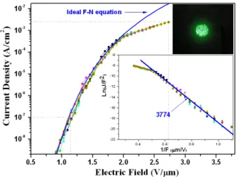
Fig. 4. Field emission properties of the well-aligned thin-MWCNTs. The top right inset shows a dark image of field emission pattern at the applied electric field of 2.7 V/μm. The bottom right inset shows the F-N plot.
we can synthesize the well-aligned thin-MWCNTs with the optimum amount of the H2S additive.
Figure 3 shows a typical Raman spectrum of the as-grown thin-MWCNTs. The Raman spectrum of thin-MWCNTs clearly indicates the appearance of the D-band at 1335.3 cm-1 and the strong G-band at 1578.1 cm-1. The G-band indicates an arrangement of the hexagonal lattice of graphite whereas the D-band indicates the level of disordered carbon. The intensity ratio of ID/IG is about 0.88. This ratio reveals that the defect level in the atomic carbon structure is low.
Figure 4 shows a typical field emission current density (J) vs. electric field (E) of the as-grown well-aligned thin-MWCNTs. Before the field emission current measurement, we performed an electrical an- nealing to obtain stable and reproducible field emis- sion performance at the current density of ~1 mA/cm2 for 1h. We repeated the field emission measurement several times. Similar J-E characteristics were ob- served regardless of which measurement, in the se- quence of measurements we performed, as shown in Figure 4, indicating that the emission current was more stabilized.
The turn-on electric field, required to obtain an emission current density of 0.1 μA/cm2 was about 1.1 V/μm. The emission current density was about 2.5 mA/cm2 at an applied electric field of 2.7 V/μm. The top right inset of Figure 4 shows a dark image of field emission pattern of the VA thin-MWCNTs at the electric field of 2.7 V/μm, presenting a little sparse field emission. The bottom right inset of Figure 4 shows the Fowler-Nordheim (F N) plot for the J-E curve of the VA thin-MWCNTs. Field emission is usually based on a F-N model [30]. The straight line indicates the field electron emission for thin-MWCNTs from quantum mechanical tunneling in a low field segment as shown in the inset of Figure 4. Since the slope of the F-N plot is inversely proportional to the field enhancement factor, the field enhancement fac- tors can be calculated using the following Eq. (1).
Slope = - B𝜙3/2/𝛾???????????????????????(1)
, where B = 6.83×10³eV-3/2Vμm-1, 𝜙?is the work function of the CNT, and 𝛾?is the field enhancement factor [31]. In the calculation of the field enhance- ment factor, the work function of the CNT was as- sumed to be equal to that of graphite (5 eV) [32]. The 𝛾?value of our VA thin-MWCNTs was calculated to be 3774, which was larger than those of the VA MWCNTs reported previously [33]. This is probably attributed to the smaller tip radius of our VA thin-MWCNTs.
There have been some reports on the field emission properties of thin-MWCNTs. Qian et al. reported field emission performances of small diameter few-walled CNT synthesized by a CCVD method using a Fe-Mo/MgO catalyst. The few-walled CNT cathode fabricated by an electrophoretic deposition method showed the current density of 10 μA/cm2 at a low turn-on field of less than 1.5 V/μm [3]. Moon et al.
studied the field emission properties of SiOx coated thin-MWNTs using a spray method which showed that the turn-on field was ~1.08 V/μm at a current of ~ 1 μA and the current density was increased to
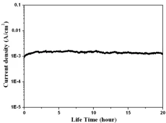
Fig. 5. Field emission stability of the well-aligned thin-MWCNTs at the emission current density of about 1 mA/cm2.
~5.8 mA/cm2 at a field of ~ 2.5 V/μm [34]. Jeong et al. investigated the field emission properties of thin-MWCNTs using a spray method. The thin-MWCNTs revealed the highest current density of approximately 1.52 mA/cm2 at 3.5 V/μm compared with DWCNTs and thick-MWCNTs [4]. When we compared the electric fields which corresponded to the emission current density of 1.0 mA/cm2 of our VA thin-MWCNTs with other results, the well-aligned thin-MWCNTs in- dicated a better field emission performance than those reported according to the very low turn-on electric field [4, 34, 35]. The field emission properties of our VA thin-MWCNTs also showed a current satu- ration-like behavior in the J-E curve. Many research groups attributed a main cause of the current satu- ration-like behavior to the interaction between neighboring CNT tips [36] or the presence of a non- metallic density of states (DOS) at the CNT tips [32], or defects on the CNT tips [37], or changes in the ad- sorbate states [38], or the voltage drop along the bulk of CNTs at the interface between the substrate and the CNTs [15]. The conventional fitting of the ideal F-N equation to the measured field emission current can be conducted on the low current segment of the reproducible J-E curve which can be obtained after the desorption of adsorbates through an electrical annealing, as shown at the straight line in F-N plot.
The J-E curve is deviated from the ideal F-N equa- tion at the high current segment. The deviation of the high current segment can be well explained by the modified F-N equation taking into consideration of the effect of voltage drop due to the bulk resistance of CNT itself and/or the contact resistance between the CNT and substrate [15, 39].
Figure 5 shows the field emission current stability of the VA thin-MWCNTs during a long lifetime meas- urement at the same initial current density of 1 mA/cm2. Then, we fixed the applied electric field for each of the CNTs for 20 h. The well-aligned thin-
MWCNTs showed a stable emission current density of over 20 h even though there was a little fluctuation in the emission current. Jeong et al. reported that the emission current density of a thin-MWCNT emit- ter, fabricated by a spray method, drastically de- creased to about 50 % after 12 h even at a relatively low initial current density of 0.19 mA/cm2 [4]. Moon et al. studied the SiOx-coated thin-MWCNTs and found that the emission current of the SiOx-coated thin-MWCNT emitter fabricated by the spray method decreased from an initial value of 110 μA/cm2 to about 55 μA/cm2 after only 2.5 h [34]. Comparing with these reports, our well-aligned thin-MWCNTs pro- vide much more excellent field emission properties especially in lower turn-on electric field and longer lifetime.
The decrease of emission current density during continuous operation could be caused by the degrada- tion of CNT tip due to Joule heating [40]. For the randomly-oriented MWCNT emitters, only the pro- truding MWCNTs can take part in the field emission, but the number of these longer MWCNTs is small. As a result, the current loading, which can be defined as the emission current per a single MWCNT, is very high, resulting in the destruction of the longer
MWCNTs during the continuous operation of the MWCNT emitters. In the other hand, uniform length of CNTs can result in a uniform distribution of field enhancement factors. Even though it’s well known that higher density of CNTs could increase the screening effect provoked by the proximity of neigh- boring tubes so as to reduce the field enhancement factor [41], we still could get a relative low but very uniformly distributed field enhancement factor from our well-aligned thin-MWCNT emitters. Therefore, uniform field enhancement factor will lead to more and uniform CNTs taking part in the field emission.
In other words, the majority of well-aligned thin-MWCNTs can participate in the field emission.
The current loading is reduced; as a result, the emis- sion current can be stable over a longer operation time. Therefore, we suggest that VA thin-MWCNTs can be used to fabricate robust field emitters for var- ious vacuum electronic devices such as field emission displays (FEDs), flat lamps, x-ray sources, and high resolution electron beam instruments.
Ⅳ. CONCLUSION
We successfully synthesized well-aligned thin- MWCNTs using a CCVD method with a H2S additive.
The as-grown CNTs were thin-MWCNTs with diame- ters of less than 10 nm and about 5 graphene layers.
The optimum H2S additive can increase the growth rate of thin-MWCNTs and induce a vertical alignment of the thin-MWCNTs. The turn-on voltage of the well-aligned thin-MWCNTs was found to be about 1.1 V/μm at a current density of 0.1 μA/cm2. The emis- sion current density was reached, 2.5 mA/cm2, at a bias field of 2.7 V/μm. Our well-aligned thin- MWCNTs also exhibited a long stability of emission current density at a emission current density of about 1 mA/cm2.
ACKNOWLEDGEMENT
This work was supported by the Seoul Fellowship.
REREFENCES
[1] A. G. Rinzler, J. H. Hanfner, P. Nikolaev, L. Lou, S. G. Kim, D. Tománek, P. Nordlander, D. T.
Colbert and R. E. Smalley, Science 269, 1550 (1995).
[2] Walt A. de Heer, A. Châtelain and D. Ugarte, Science 270, 1179 (1995).
[3] C. Qian, H. Qi, B. Gao, Y. Cheng, Q. Qiu, L. Qin, O. Zhou and J. Liu, J. Nanosci and Nanotec. 6, 1 (2006)
[4] H. J. Jeong, H. K. Choi, G. Y. Kim, Y. I. Song, Y. Tong, S. C. Lim and Y. H. Lee, Carbon 44, 2689 (2006).
[5] M. S. Dresselhaus, G. Dresselhaus and P. Avouris, eds., Carbon Nanotubes: Syntheis, Structure, Properties, and Applications, Springer-Verlag, Heidelberg (2000), Vol.80.
[6] S. Fan, M. G. Chapline, N. R. Franklin, T. W.
Tombler, A. M. Cassell and H. Dai, Science 283, 512 (1999).
[7] A. Modi, N. Koratkar, E. Lass, B. Wei and P. M.
Ajayan, Nature 424, 171 (2003).
[8] K. Hata, D. N. Futaba, K. Mizuno, T. Namai, M.
Yumura. S. Iijima, Science 306, 1362 (2004).
[9] H. Nishino, S. Yasuda, T. Namai, D. N. Futaba, T. Yamada, M. Yumura, S. Iijima and K. Hata, J.
Phys. Chem. C 111, 17961 (2007).
[10] T. Hiraoka, T. Yamada. K. Hata, D. N. Futaba, H.
Kurachi, S. Uemura, M. Yumura and S. Iijima, J.
Am. Chem. Soc. 128, 13338 (2006).
[11] T. Yamada, T. Namai, K. Hata, D. N. Futaba, K.
Mizuno, J. Fan, M. Yudasaka, M. Yumura and S.
Iijima, Nat. Nanotechnol. 1, 131 (2006).
[12] K. S. Kim, J. H. Ryu, C. S. Lee, H. E. Lim, J.
S. Ahn, J. Jang and K. C. Park, J. Korean Vac.
Soc. 17, 90 (2008).
[13] E. C. Choi, J. T. Kim, Y. S. Park, W. S. Choi and B. Hong, Korean Vac. Soc. 16, 187 (2007).
[14] M. Chhowalla, C. Ducati, N. L. Rupesinghe, K. B.
K. Teo and G. A. J. Amaratunga, Appl. Phys. Lett.
79, 2079 (2001).
[15] E. Minoux, O. Groening, K. B. K. Teo, S. H. Dalal, L. Gangloff, J.-P. Schnell, L. Hudanski, L. Y. Y.
Bu, P. Vincent, P. Legagneux, G. A. J. Amaratunga and W. I. Milne, Nano. Lett. 5, 2135 (2005).
[16] R. G. Forbes, C. J. Edgcombe and U. Valdre, Ultramicroscopy 95, 57 (2003).
[17] H. M. Cheng, F. Li, G. Su, H. Y. Pan, L. L. He, X. Sun and M. S. Dresselhaus, Appl. Phys. Lett.
72, 3282 (1998).
[18] H. Ago, T. Komatsu, S. Ohshima, Y. Kuriki and M. Yumura, Appl. Phys. Lett. 77, 79 (2000).
[19] L. Ci, Z. Rao, Z. Zhou, D. Tang, X. Yan, Y. Liang, D. Liu, H. Yuan, W. Zhou, G. Wang, W. Liu and S. Xie, Chem, Phys. Lett. 359, 63 (2002).
[20] E. H. Hong, K.-H. Lee, S. H. Oh and C.-G. Park, Adv. Mater. 14, 676 (2002).
[21] Y. Saito, T. Nakahira and S. Uemura, J. Phys.
Chem. B 107, 931 (2003).
[22] J. Wei, L. Ci, B. Jiang, Y. Li, X. Zhang, H. Zhu, C. Xu and D. Wu, J. Mater. Chem. 13, 1340 (2003).
[23] L. Song, L. Ci, L. Lv, Z. Zhou, X. Yan, D. Liu, H. Yuan, Y. Gao, J. Wang, L. Liu, X. Zhao, Z.
Zhang, X. Dou, W. Zhou, G. Wang, C. Wang and S. Xie, Adv. Mater. 16, 1529 (2004)
[24] A. J. Hart and A. H. Slocum, J. Phys. Chem. B 110, 8250 (2006).
[25] L. Ci, S. M. Manikoth, X. Li, R. Vajtai and P. M.
Ajayan, Adv. Mater. 19, 3300 (2007).
[26] T. Inoue, I.GunjishimaandA.Okamoto, Carbon 45, 2164 (2007).
[27] H. Zhang, G. Cao, Z. Wang, Y. Yang, Z. Shi and Z. Gu, J. Phys. Chem. C 112, 4524 (2008).
[28] G. G. Tibbetts, C. A. Bernardo, D. W. Gorkiewicz and R. L. Alig, Carbon 32, 569 (1994).
[29] M. S. Kim, N. M. Rodriguez and R. T. K. Baker, J. Catalysis 143, 449 (1993).
[30] R. H. Fowler and L. W. Nordheim, Proc. R. Soc.
London, Ser. A 119, 173 (1928).
[31] R. G. Forbes, Solid-State Electron. 45, 779 (2001).
[32] J.-M. Bonard, J.-P. Salvetat, T. Stöckli, W. A. de Heer, L. Forró, A. Châtelain, Appl. Phys. Lett. 73, 918 (1998).
[33] M. Sveningsson, R.-E. Morjan, O. A. Nerushev, Y.
Sato, J. Bäckström, E. E. B. Campbell and F.
Rohmund, Appl, Phys. A. 73, 409 (2001).
[34] J. S. Moon, P. S. Alegaonkar, J. H. Han, T. Y.
Lee, J. B. Yoo and J. M. Kim, J. Appl. Phys. 100, 104303 (2006).
[35] R. Seelaboyina, J. Huang and W. B. Choi, Appl.
Phys. Lett. 88, 194104 (2006).
[36] P. G. Collins and A. Zettl, Appl. Phys. Lett, 69, 1969 (1996).
[37] X. Xu and G. R. Brandes, Appl. Phys. Lett. 74, 2549 (1999).
[38] K. A. Dean and B. R. Chalamala, Appl. Phys. Lett.
76, 375 (2000).
[39] S. H. Jo, Y. Tu, Z. P. Huang, D. L. Carnahan, J.
Y. Huang, D. Z. Wang and Z. F. Ren, Appl. Phys.
Lett. 84, 413 (2004).
[40] S. C. Lim, Y. C. Choi, H. J. Jeong, Y. M. Shin, K. H. An, D. J. Bae, Y. H. Lee, N. S. Lee and J. M. Kim, Adv. Mater. 13, 1563 (2001).
[41] L. Nilsson, O. Groening, C. Emmenegger, O.
Kuettel, E. Schaller, L. Schlapbach, H. Kind, J.-M.
Bonard and K. Kern, Appl. Phys. Lett. 76, 2071 (2000).
촉매 화학 기상 증착법을 사용하여 실리콘 기판위에 수직 정렬된 직경이 얇은 다중층 탄소나노튜브의 합성과 그들의
전계방출 특성
정승일, 최상규, 이승백*
한양대학교 나노반도체공학과, 서울 133-791
(2008년 6월 2일 받음, 2008년 7월 7일 수정, 2008년 7월 8일 확정)
최적화된 량의 황화수소 첨가 가스를 이용하여 실리콘 기판위에 증착된 Fe/Al 박막위에 촉매 화학 기상 증착법을 사용하여 직 경이 얇은 다중층 탄소나노튜브가 수직 정렬되어 합성되었다. 주사전자현미경 관측 이미지에서 합성된 탄소나노튜브는 상대적 으로 일정한 길이를 가지고 기판에 수직으로 정렬되었다. 투과전자현미경 관측에서 합성된 탄소나노튜브는 10nm 이내의 작은 외경을 가졌고 촉매가 거의 없었다. 평균 튜브의 벽 수는 약 다섯 개이다. 수직 정렬된 직경이 얇은 다중층 탄소나노튜브의 성장 메카니즘이 제시되었다. 수직 정렬된 직경이 얇은 다중층 탄소나노튜브는 0.1 μA/cm2의 전류밀도에서 약 1.1 V/μm 낮 은 턴-온 전계를 나타내었고 2.7 V/μm의 전계에서 약 2.5 mA/cm2의 전류밀도를 얻었다. 게다가, 수직 정렬된 직경이 얇은 다중층 탄소나노튜브는 약 1 mA/cm2의 전류밀도에서 20시간동안 전류밀도 저하 없이 좋은 전계 방출 안정성을 보여주었다.
Keywords : 직경이 얇은 다중층 탄소나노튜브, 촉매 화학 기상 증착법, 전계 방출
* [E-mail] : [email protected]