Vol. 19, No. 3, pp. 5-10, June 2015
Structural Analysis of a Cavitary Region Created by Femtosecond Laser Process
Takaaki Fujii†, Kenji Goya* and Kazuhiro Watanabe
(Received 29 December 2014, Revision received 7 October 2015, Accepted 10 April 2015)
Abstract: Femtosecond laser machining has been applied for creating a sensor function in silica glass optical fibers. Femtosecond laser pulses make it possible to fabricate micro structures in processed regions of a very thin glass fiber line because femtosecond laser pulses can extremely minimize thermal effects.
With the laser machining to optical fiber using a single shot of 210-fs laser at a wavelength of 800 nm, it was observed that a processed region surrounded a thin layer which seemed to be a hollow cavity monitored by scanning electron microscopy (SEM). This study aims at a theoretical investigation for the processed region by using a numerical analysis in order to embed sensing function to optical fibers.
Numerical methods based finite element method (FEM) has been used for an optical waveguide modeling.
This report suggests two types modeling and describes a comparative study on optical losses obtained by the experiment and the numerical analysis.
Key Words:Femtosecond Laser, Numerical Analysis, FEM, Refractive Index, Optical Fiber Sensor.
*† Takaaki Fujii (corresponding author), Kenji Goya and Kazuhiro Watanabe : Department of Information System Science, Soka University.
E-mail : [email protected], Tel : +81-42-691-8197
1. Introduction
Recently, it is a major problem for social to distort and collapse by aged deterioration of building. Because serious accidents occur such as depression of road in Korea and collapse of tunnel in Japan, psychological stress and damage scale up for people. It is important for avoiding accidents to develop environmental monitoring.
Electrical system already has used for such problems. However, the system has some problems such as high consumption power and a short life-span. In order to reduce power consumption, sensors system with optical fiber sensors is expected
and advanced for optical monitoring system.
Because fiber optic sensor need no power source at the sensor portion to drive sensing, an installation and measurement are flexibly possible at various places. Fiber optic element is also better than electric cable for immunity to electromagnetic induction, corrosion resistance. Furthermore, an optical fiber has advantages such as lightweight and being thin material. Optical fiber shows the utility by these characteristics, various fiber optic sensors are consequently developed. Bending sensors using optical fiber have been developed by laser irradiation such as FBG and LPFG. These sensors using photo-induced refractive index (RI) changed that an optical fiber is irradiated with ultraviolet ray are modulated periodically core RI. Periodic structure perform spectrum filter because light attenuation occurs due to mode coupling or Bragg reflection. Optical transfer characteristics of its
sensor change by modulation cycle and RI distribution. However, these sensors need temperature compensating. Accordingly, measurement is much less accurate in inhospitable environment.
So development of another technique is made a suggestion. Conventional technique is roughly defined as Type I and new technique is named Type II. Sensor part of Type II (usually consisted of a permanent processed region) is made by arraying a cavitary region (void) for internal optical fiber using femtosecond laser micromachining. Type II reduces temperature dependency to weak point of Type I. However, Type II has different weaker point in contrast to Type I. This sensor has poor sensitivity because bending peak decrease due to Mie scattering. Subsequently it is difficult for making reproducibility because the sensor fabrication needs accuracy in the scale of nanometer.
Our work approaches development of bending sensor using Mie scattering by void creation inside an optical fiber using a femtosecond laser. In the femtosecond regime, the laser energy can be immediately absorbed by a very fast multi-photon absorption less than thermal diffusion-time scale, which induces a non-thermal equilibrium condition between electrons and ions. With the laser machining to optical fiber, it was observed that a processed region surrounded a thin layer which seemed to be a hollow cavity monitored by scanning electron microscopy (SEM). In this work, in order to clarify the refractive index (RI) of the void, theoretical examination and numerical calculation will be shown. Accurate modeling of analysis object has been necessary for the simulation. Specifically it is important to model the shape of the processed region and the value of RI.
It is considered that the RI of the thin layer would be higher than the RI of void or optical fiber. This report suggests two types modeling, where one of the models has two parts of void and thin layer for the processed region. The other hand is that an
effective RI is defined by taking the average of the void area and thin layer. These models are analyzed by finite element method and this report shows analytical results.
2. Numerical Analysis
2.1 Finite Element Method (FEM)
The FEM is one of a typical method for numerical electromagnetic field analysis. After a computational domain separated by some elements (meshes) surrounded arbitrary points, Maxwell equation is calculated at each of them. Moreover, a weighted residual method is used to accurately discretize the equation. There is a weighting function such as Galerkin method1). It also takes account of boundary condition. The FEM gets finally large-scale simultaneous linear equations2) and it solves using direct method or iteration method.
Direct method uses Gaussian elimination however the calculation time is usually long because of increasing the calculation amount. On the other hand, iteration method3) calculates by Jacobi method and so on. Calculation time is usually shorter than direct method because iteration method less than direct method about the calculation amount.
However it is possible that solution doesn’t converge.
2.2 Boundary Conditions
In electromagnetic field analysis, simultaneous differential equations with two unknowns that are electric and magnetic field must be solved. Using the FEM, differential equation with one unknown can be gotten by eliminating either of their field.
This differential equation is called Helmholtz equation4). It’s necessary to set the boundary conditions for calculating its equation. Boundary conditions are given outside computational domains.
The computational results depend on boundary
Boundary condition FIM MWAVE Features
Dirichlet Electric wall Electric field is vertical direction perpendicular to boundary Neumann Eagnetic wall M agnetic field is vertical direction perpendicular to boundary
Robin Impedance Pairing Dirichlet with Neumann boundary condition Periodic Periodic Decreasing calculation area by periodic structure Transparent Tansparent Can transparent without reflection at boundary Table 1 Boundary condition features.
condition. For example, incorrect boundary conditions give physically unnatural results. On the other hand, if correct boundary conditions are set, the calculation time and file size may be decreased.
There are five main types of boundary conditions (Table 1). They are fixed boundary condition (Dirichlet boundary condition), natural boundary condition (Neumann boundary condition), third type boundary condition (Robin boundary condition), periodic boundary condition and transparent boundary condition. In used software for this analysis, configurable boundary conditions select from electric wall, magnetic wall, impedance boundary condition, periodic boundary condition and transparent boundary condition. It is installed E (electric field) and H (magnetic field) to boundary condition understand (Fig. 1).
Electromagnetic wave direction E
H
Fig.1 Electromagnetic field distribution and wave
Perfect electric conductor
E H
E H x
z
y
Fig. 2 Reflection at perfect electric conductor
Electric wall corresponds to Dirichlet boundary condition. Electric field is distributed to tangential direction at boundary and set zero at boundary.
Therefore electric wall means perfect electric conductor (Fig. 2). Magnetic wall corresponds to Neumann boundary condition. Magnetic field is distributed to tangential direction at boundary and set zero at boundary. Therefore magnetic wall means perfect magnetic conductor. Impedance boundary condition corresponds to third type boundary condition, pairs Dirichlet with Neumann boundary condition, and can treat frequency dispersive conductor5). Periodic boundary condition is used in cases of electromagnetic field distribution cycle through rotation or translation direction and can decrease calculation area. Used periodic boundary condition, simulation run only compartment area. About electromagnetic field in overall area, compartment area by simulation cycle through periodic direction. Transparent boundary condition is transmitted electromagnetic wave that runs outward analysis area, and establishes wave propagation without reflection at boundary6).
3. Experimental Setup
A Ti:sapphire laser system to optical fiber using a single shot of 210-fs laser at a wavelength of 800nm is used in the experiments to fabricate the void. It was observed that a thin layer surrounded the processed region which seemed to be a hollow cavity by means of scanning electron microscopy (SEM). The numerical calculation was made on
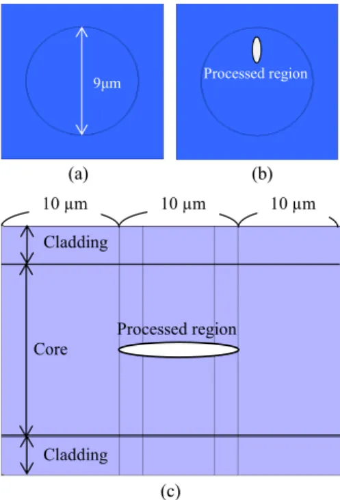
FIMMWAVE of analysis software and FIMMPROP of its extended software. Numerical analysis method uses FEM and analysis model set boundary conditions that are electric wall at both sides and magnetic wall at up to bottom in computational domain (Fig. 3). A single mode optical fiber used in this study has core and cladding diameter are 9µm and 125µm, respectively. Note that the model
Magnetic wall
Magnetic wall
Electric wall Electric
wall
Cladding Core
Void
Fig. 3 Optimum boundary conditions
9μm Processed region
(a) (b)
Core
Processed region
Cladding Cladding
10 µm 10 µm 10 µm
(c)
Fig. 4 The modeled structure The cross-sectional view of
(a) optical fiber and (b) sensing portion.
(c) The longitudinal view of sensor portion.
should be limited in computational domain around core part because the analysis result becomes much more accurate(Fig. 4 (a)). The RI of core and cladding are 1.4514 and 1.4469, respectively. Beside, processed region position gets closer to the center of the fiber core with an interval of 1µm (Fig. 4 (b)).
Fig. 4 (c) shows optical fiber model involved sensor part. The two types of model will be suggested, one of which has two layers structure consists of void and thin layer with RI of 1.50 (Fig. 5 (a)). The void model size sets W0.17×D10.00×H2.00µm and RI value is 1.00. Thin layer size was set to 50nm around the void. The other modeling is the composite structure with void and thin layer that set effective RI (Fig.5 (b)). The composite structure model size sets W 0.20 × D 10.00 × H 2.00 µm.
Void
Thin layer
Void and thin layer
Fig. 5 The two types models of processed region.
(a) Two layers structure of void and thin layer.
(b) Composite void with athinlayer
4. Analysis Result
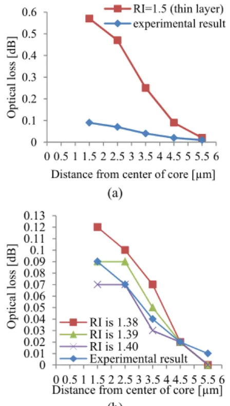
Fig. 6 shows the optical loss with varying the position of the processed region. Comparing the experiment and analytical result, the optical losses in the case of Fig. 5 (a) is in disagreement with the experiment [see Fig. 6 (a)] because the number of the mushes is inefficient to construct the layer.
Taking a look at Fig. 6 (b) regarding to Fig. 5 (b), the effective RI value is varied between 1.35 and 1.45. When effective RI set to a range of 1.38-1.40, the calculation shows a good agreement with the experimental result. The optical loss is slightly
larger than experimental result at RI=1.38. For RI=1.39~1.4, the optical losses becomes closer than the case of 1.38.
0 0.1 0.2 0.3 0.4 0.5 0.6
0 0.5 1 1.5 2 2.5 3 3.5 4 4.5 5 5.5 6
Optical loss [dB]
Distance from center of core [µm]
RI=1.5 (thin layer) experimental result
(a)
0.010 0.020.03 0.040.05 0.060.07 0.080.090.1 0.110.12 0.13
0 0.5 1 1.5 2 2.5 3 3.5 4 4.5 5 5.5 6
Optical loss [dB]
Distance from center of core [µm]
RI is 1.38 RI is 1.39 RI is 1.40 Experimental result
(b)
Fig. 6 Comparison to reflective index in optical loss.
(a) Two layers structure.
(b) The composite structure.
5. Conclusion
This report models two types processed region and analyzes mode in waveguide with analysis software and represents analytical results.
For analysis results, two layers structure model isn’t enough about the number of meshes. Therefore the optical loss is very different as processed region position is closer and closer to center of the core.
Model of the processed region in complex with void and thin layer that set an effective RI approaches the experimental result in effective RI = 1.38~1.40.
Effective RI seems to be obtained by these
analytical results using some theories. Effective medium approximation7) could be proposed as one of the theories, in which the applicable condition would be limited for an object size that is shorter than the wavelength of incident light.
This report suggests two types processed region models. It is necessary to consider the optimum model for constructing actual optical fiber sensor.
Acknowledgement
This work has been supported by JSPS KAKENHI Grant Numbers 24510126.
References
1. A. Maruta, 1994, “Transparent Boundary for Finite-Element Beam-Propagation Method”, The Institute of Electronics, Information and Communication Engineers, Vol.J77-C-1, No. 2, pp. 35-40.
2. T. Hosono and K. Tanaka, 2009, “Progress and Perspective in Electromagnetic Theory – Some Problems in Electromagnetic Theory and Numerical Techniques in Computational Electromagnetics”, The Institute of Electronics, Information and Communication Engineers, Vol.J92-C (8), pp. 314-324.
3. T. Fujisawa and M. Koshiba, 2002, “Full-Vector Finite-Element Beam Propagation Method for Three-Dimensional Nonlinear Optical Waveguides”, The Institute of Electronics, Information and Communication Engineers, Vol.J85-C, No. 6, pp. 440-448.
4. K. Nagaya and K. Poltorak, 1988, “Method for Solving Eigenvalue Problems of Helmholtz’s Equation Having a Circular Outer and a Number of Eccentric Circular Inner Boundaries”, Transactions of the Japan Society of Mechanical Engineers, Vol. 54, pp. 2815-2821.
5. M. Takata, 2002, “A Study on Conductor Surface Impedance Boundary Condition on FDTD Method”, IEICE, 13.
6. A. Maruta, 1994, “Transparent Boundary for Fnite-Elemtnt Beam-Propagation Method”, IEICE, Vol. 77, pp. 35-40.
7. S. Kawabata, 1997, “Determination of the Film Thickness and the Effective Medium Approximation Theories in Ellipsometry”, Journal of the Surface science society of Japan, Vol. 18, No. 11, pp. 681-686.