http://dx.doi.org/10.46670/JSST.2021.30.4.218 pISSN 1225-5475/eISSN 2093-7563
Designing a nanocrystal-based temperature and strain multi-sensor with one-step inkjet printing
Junsung Bang
1, Junhyuk Ahn
1, and Soong Ju Oh
1,+Abstract
Wearable multi-sensors based on nanocrystals have attracted significant attention, and studies on patterning technology to implement such multi-sensors are underway. Conventional patterning processes may affect material properties based on high temperatures and harsh chemical conditions. In this study, we developed an inkjet printing technique that can overcome these drawbacks through the appli- cation of patterning processes at room temperature and atmospheric pressure. Nanocrystal-based ink is used to adjust properties effi- ciently. Additionally, the viscosity and surface tension of the solvents are investigated and optimized to increase patterning performance.
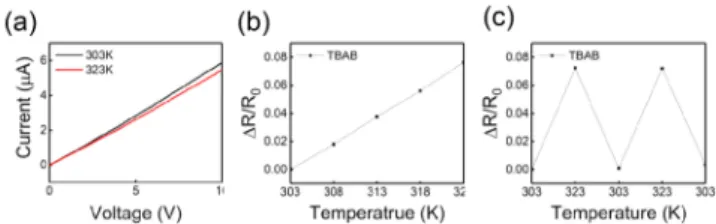
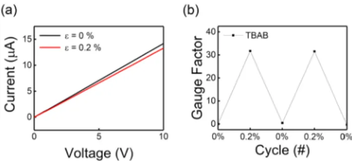
In the patterning process, the electrical, electrothermal, and electromechanical properties of the nanocrystal pattern are controlled by the ligand exchange process. Experimental results demonstrate that a multi-sensor with a temperature coefficient of resistance of 3.82 × 10
−3K
−1and gauge factor of 30.6 can be successfully fabricated using one-step inkjet printing.
Keywords : Nanocrystal, Inkjet printing, One-step, Surface chemistry, Ligand exchange, Multi-sensor.
1. INTRODUCTION
The development of various electronic devices [1,2], such as wearable multi-sensors [3–8], based on nanoparticles is well underway. Accordingly, circuit patterning technology is in high demand to facilitate the development of various multi-sensors.
Modern patterning techniques include a photolithography process using photoresist materials and a thermal deposition process.
However, these methods are complex and require expensive equipment. In this study, to overcome the disadvantages of the patterning processes mentioned above, a one-step patterning process using inkjet printing was developed.
In inkjet printing, the process of printing patterns on substrates using colloidal nanocrystal (NC) ink is not only mask-free, on- demand, and requiring no contact with materials, but it is also cheap and fast advantages because this process involves directly converting digital images into substrates. Additionally, NCs can be used as ink because they are surrounded by organic shells
(ligands) that are easily dispersed in non-polar solvents.
Furthermore, NCs have been applied to various temperature, strain, and pressure wearable sensors [9–13] because their properties can be adjusted by controlling the surface ligand exchange process based on their large surface-to-volume ratio.
In this work, based the characteristics described above, NC colloidal ink was printed and patterned directly on a substrate to fabricate multi-sensor arrays. Subsequently, a ligand exchange process was conducted to adjust the electrical, electrothermal, and electromechanical properties of the fabricated NC patterns, as well as the inter-particle distances between NCs. Therefore, the conduction mechanisms [14] of NC thin films can be controlled by the ligand exchange process. In this manner, temperature and strain sensors can be fabricated. In this study 300 μm linewidth sensor patterns were successfully developed using inkjet printing, demonstrating that this technology can contribute to the manufacturing of next-generation devices, such as smart wearable healthcare systems.
2. EXPERIMENTAL SETUP
2.1 Materials
Oleic acid (OA, 90%), oleylamine (OAm, 70%), tetrabutylammonium bromide (TBAB, ≥99%), toluene (99.8%), ethanol (≥99.5%), octane (99+%), isopropanol (99.5%), and (3-
1
Department of Materials Science and Engineering, Korea University 145, Anam-ro Seongbuk-gu, Seoul 02841, Republic of Korea
+