A Link Layer Design for DisplayPort Interface
Hyun-Bae Jin * , Kwang-Hee Yoon ** , Tae-Ho Kim * , Ji-Hoon Jang * , Byung-Cheol Song * , Jin-Ku Kang *
★Abstract
This paper presents a link layer design of DisplayPort interface with a state machine based on packet processing. The DisplayPort link layer provides isochronous video/audio transport service, link service, and device service. The merged video, audio main link, and AUX channel controller are implemented with 7,648 LUTs(Loop Up Tables), 6020 register, and 821,760 of block memory bits synthesized using a FPGA board and it operates at 203.32MHz.
Key words: DisplayPort, Main Link, Auxiliary channel (AUX channel), DisplayPort Configuration Data(DPCD), Extended Display Identification Data(EDID), Digital Visual Interface(DVI)
* School of Electronics Engineering, Inha University
** Silicon Works Co., Ltd.
★
Corresponding author※ Acknowledgment
This work is supported by Human Resource Training Project for Strategic Technology from the Ministry of Knowledge Economy (MKE) and Korea Institute for Advancement of Technology (KIAT).
Authors also thank IDEC for its hardware and software assistance.
Manuscript received Dec. 3, 2010 ; revised Dec. 29, 2010
I. Introduction
DisplayPort is an open industry standard digital display interface suggested by the Video Electronics Standards Association (VESA) [1],[2]. DisplayPort is designed to serve widespread connection solutions for PCs, monitors, panels, projectors, and high definition display applications. DisplayPort consolidates internal and external connection methods to reduce device complexity and provides performance for the next generation of displays featuring higher color depths, refresh rates, and display resolutions.
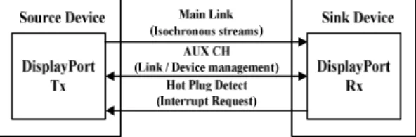
DisplayPort connections consist of main link, AUX channel, and Hot Plug Detect (HPD) signal line.
Fig. 1 shows transport channels of source and sink device of DisplayPort. The main link is a
uni-directional, high-bandwidth channel used to transport isochronous data streams such as uncompressed video and audio data. AUX channel is a half-duplex bidirectional channel used for link management and device control. The HPD signal serves as an interrupt request from the Sink Device.
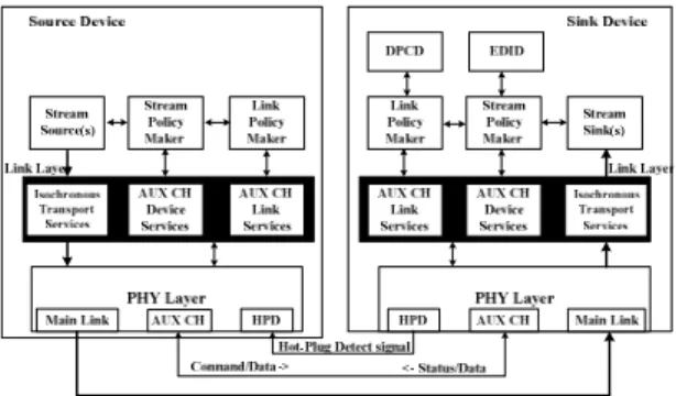
Fig. 2 shows the layered architecture of DisplayPort. DPCD in the sink device contains the capability of receiver and link status information.
EDID memory describes the monitor maker, production data and supporting resolution of the monitor. Link and stream policy makers manage the link and stream, respectively.
In this paper, a design of DisplayPort link layer with a state machine based packet processing is described. First, the main link design for video/audio data transmission and receiving is described. And then the AUX channel design is given. In section IV, experimental results of the prototype are presented.
Fig. 1. DisplayPort Structure
Fig. 2. Block Diagram of DisplayPort.
II. DESIGN OF DISPLAYPORT MAIN LINK
The main link is a uni-directional, high-bandwidth channel used to transport isochronous data streams such as uncompressed video and audio data. The stream data (video and audio) are packed into“micro-packets” which are called “transfer units”.
The transfer unit length is 32 to 64 link symbols per lane. After the stream data is packed and mapped to the main link, the packed stream data rate will be equal to or less than the link symbol rate of the main link. When the stream data rate is less than the link symbol rate, stuffing symbols are inserted. During the horizontal and vertical blanking period of the main video stream, the link symbols are almost filled with stuffing symbols. They may be substituted with a stream attribute packet used for regenerating the stream in the sink device, and optional secondary-data packets such as audio stream packets.
1. Main link transmitter for video signal
Fig. 3 shows the designed block diagram of the video transmitter via main link. It is composed of lane decision, data enable (DE) generator, link data synchronizer, FIFOs, bus steering block, FIFO packed data, lane data generator and interlane skew insertion blocks. Since the test board receives the data as DVI format, the DVI Rx block is included for DisplayPort Tx verification. Lane decision and DE Generator blocks receive the video data synchronized with HSYNC, VSYNC and data enable (DE) signal from the DVI pattern generator block or DVI RX signal. The main purpose of the lane decision block is to determine TU (Transfer Units)size and number of lanes from video data and the DE generator block makes a line delay of the DE signal coming from the DVI Rx block. The link layer has two different time domains, which are the pixel clock depending on video resolution and frame rate and the link symbol clock domain at 162MHz or 270MHz. Thus the three stages of FIFO are inserted to match timing between two different time domains. The first FIFO is an asynchronous FIFO to transfer data between two time domains. The second FIFO is the bus steering FIFO to assign the data to suitable lanes among four lanes. The third FIFO is for packetizing the data to DisplayPort data format. The following lane data generator block is for placing the relevant symbols at the allocated part of packetized data. The main link transmitter interface adapts the 8B/10B encoding as its channel coding scheme to provide symbol-level DC balancing. The output of the 8B/10B encoder is provided to the scrambler.
Fig. 3. Designed main link transmitter for video signal
2. Main link receiver for video signal
The designed main link video receiver is shown in Fig. 4. It is composed of 8B/10B decoder, parallel descrambler, interlane deskew block, stream attribute recovery, stream unpacker, bus steered FIFO, and time based converter (TBC) block. The receiver decodes, deskews, unpacks, unstuffs, and unframes the data coming from the transmitter after the data from transmitter are decoded by the 8B/10B decoder and the descrambler. The main stream attribute recovery block interprets video, timing and stream format from the packetized data. The main stream unpacker block regenerates the original RGB dataand frame symbol. The recovered stream data are transferred to the bus steered FIFO and the time based converter (TBC) for display. The TBC block converts the time domain between the link symbol clock domain and the stream clock domain.
Additional blocks are designed for verification of the main link video receiving with DVI format display.
The restored RGB video data are synchronized with DVI timing signals (HSYNC, VSYNC, DE) by timing generator and FIFO read/write control. The final output data are provided to a monitor being operated by DVI format.
8B/10B Decoder
Parallel Descramber
Interlane Deskew Insertion
Main Stream Attribute Recovery
Main Stream Unpacker
FIFO Read Control
FIFO Bus Steering
FIFO Write Control
Time Gen
&
FIFO Read Control
TBC (Time Base Converter) FIFO FIFO Write Control Main Stream Data (Htotal, Vtotal,Hsw,Vsw,etc,)
To Link
HSYNC,VSYNC, DE
DVI Tx Chip RGB
DVI Tx
Fig. 4. Designed main link receiver for video signal
3. Main link transmitter for audio signal
Fig. 5 shows the designed main link audio transmitter for DisplayPort. For test, the audio Tx takes audio stream data of SPDIF format output [3]-[5]. The secondary data source block converts SPDIF format into DisplayPort audio format. In DisplayPort, audio stream data is the secondary data packet, which consists of InfoFrame packet, audio timestamp packet, and audio stream packet.DisplayPort must comply with CEA-861C standard when using InfoFrame. InfoFrame packet consists of audio cording type, audio channel count, sampling frequency, sample size, and speaker position, etc.
InfoFrame packet must be sent once per frame during the vertical blanking period of the main video stream. The audio timestamp packet consists of Maud23:0 and Naud23:0. The relationship of Maud and Naud is that Maud/Naud = 512 * fs / f_LS_clk, where fs is the sampling frequency of the audio stream and f_LS_clk is the link symbol clock.
The audio timestamp packet is transported once per main video stream horizontal line period. The audio stream packets are sent during both horizontal and vertical blanking periods of the main video stream.
Fig. 5. Designed main link transmitter for audio signal All of the audio data packet must be protected via error correcting code (ECC). The audio data packet consists of a header protected by four bytes of parity, followed by a 16 byte payload data protected by four bytes of parity. The audio data packet ends with a parity byte. Audio packets constructed with less than 16 bytes of data use zero padding to fill the remaining data positions. DisplayPort adopts the Reed- Solomon code, RS(15,13), with a symbol size of one nibble(four bits) in the ECC block. Also, in order to enhance the error correcting capability, the ECC block incorporates nibble interleaving after the error correction encoding. Combining RS(15,13) with the nibble interleaving, the ECC block is capable of correcting up to two byte error in a 16 byte data block.
4. Main link receiver for audio signal
Fig. 6 shows the block diagram of the designed audio receiver. The packed audio data comes from the secondary data packer in transmitter. The secondary data unpacker block unpacks audio stream data and the ECC block corrects received audio data error. The secondary data sink block converts DisplayPort audio stream format into SPDIF format for test.Fig. 6. Designed main link receiver for audio signal The Reed Solomon decoder consists of syndrome computation block, key equation solver block, Chien search and Forney algorithm blocks, and FIFO.
Syndrome computation block calculates the syndrome polynomial containing error patterns using roots of the generator polynomial. The key equation block performs computation to solve the key equation, which the error value and the error locator polynomial can be obtained. Chien search and Forney algorithm blocks detect the error locations and calculate the error values. The FIFO in the RS decoder is used to delay the received symbols according to the latency. The decoder corrects received error symbols by adding the delayed FIFO outputs to error values.
5. Merging the video and audio data
Fig. 7 shows the block diagram of merged video and audio for main link. The video and audio data come from DVI RX and SPDIF RX converts into DisplayPort format. The lane data generator block merges audio and video data. The merged video and audio data goes through the physical layer of transmitter and receiver. The physical layer Tx and Rx chips are designed separately for the link layer design verification. The interlane deskew insertion block in the receiver separates video and audio data in the receiver. The received video data goes to DVI Tx block to display and the audio data goes SPDIF format transmitter to generate sound in the speaker.Fig. 7. Block diagram of merged video and audio signal for main link
III. DESIGN OF DISPLAYPORT AUXILIARY CHANNEL (AUX CHANNEL)
1. DisplayPort AUX channel operation
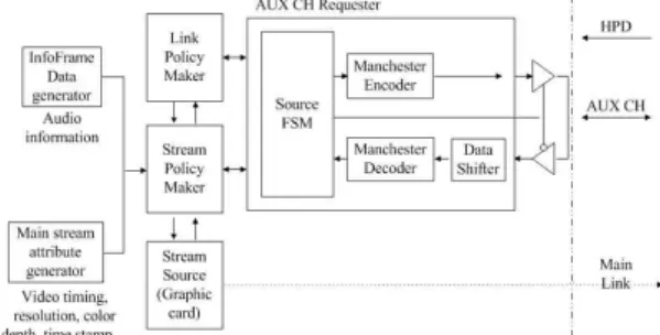
The AUX channel provides 1Mbps data rate and uses Manchester II channel coding to enhance the reliability of data transfer. The AUX channel clock is extracted from the data stream and the transaction of AUX channel is started by the source device. The sink device makes the AUX channel interact with the source device by toggling the HPD signal and sending IRQ to source device. The AUX channel physical interface uses a single differential pair carrying self-clocking data. All transactions must start with a preamble “SYNC” for synchronizing the requester (source device) and the replier (sink device), and must end with a “STOP”.AUX channel syntaxes have two categories. One category is the native AUX channel syntax for reading or writing DPCD. the other one is for mapping of I2C onto the AUX channel for EDID. A four bit command, COMM3:0, must be transmitted after the preamble, followed by a 20bit address, ADDR19:0. The DisplayPort capability, status and control function are directly mapped to the 20bit address space. In order to transfer isochronous data stream from source device to sink device, the following process is executed. The source device initializes the link by reading the link capability field of DPCD. The link capability field represents the performance of the receiver in sink device. The performance of the receiver includes the maximum bit rate and the maximum number of lane of main link.
Link policy maker starts link training and transmits the data to the sink device and informs the link configuration to the sink device. At the
same time, link policy maker transfers the result of link training to stream policy maker. The state of current link and receiver’s performance is recognized while initializing the link. For this reason, source device reads the link configuration field of the DPCD and the source finite state machine (FSM) of AUX channel requester receives command, address, and data from link policy maker. And then the data is read or written to DPCD memory. Outputs of the source FSM are encoded with Manchester II in order to transfer data to AUX channel replier.
Manchester II coding method is implemented to recover the clock easily when the data is receiving.
But it is needed alternative mechanism since input data is missed at the Manchester II decoder block when a phase of the signal is changed by AUX channel cable. Therefore, AUX CH physical layer needs to adjust the phase of the data according to the received clock. Manchester II decoder of AUX CH replier decodes the delayed data and sends them to sink FSM. The sink FSM extracts command, address and data from decoded data.
2. Designed source device for AUX channel
Fig. 8 shows the designed source device structure for AUX channel. The source device consists of InfoFrame data generator, main stream attribute generator, stream source, link policy maker and stream policy maker.Fig. 8. Source device for AUX channel.
Link policy maker performs the manin link training, maintenance and link configuration. Fig. 9 shows the state diagram of the link training FSM.
The link training consists of main link disable state, clock recovery pattern state, channel equalization state, and normal operation state.
Fig. 9. Link training procedure.
Each state is determined by the data value of specified DPCD address. The main link is reorganized when the state of link training is changed by data transition between the source device and the sink device. When link training state is normal operation state, the main link transmits the stream data from the source device to the sink device.
3. Designed sink device for AUX channel
Fig. 10 shows the sink device structure for AUX channel. The sink device consists of link policy maker, stream policy maker, EDID memory and DPCD memory. The main link status and capability are stored in DPCD. The sink device capability is stored in EDID. The sink FSM transmits the extracted data to DPCD memory wrapper, and if all data was stored or prepared to read memory, DPCD memory wrapper responds AUX_ACK signal to source device. If write operation is not supported, it transmits AUX_NACK signal. When the memory is not prepared to read or write, the source device tries again.Fig. 10. Sink device for AUX channel.
IV. EXPERIMENTAL RESULTS
Fig. 11 shows the designed DisplayPort link layer verification system. In this verification system, DVI Tx and Rx blocks are inserted to handle the data via DVI Port. The simulation result of DisplayPort main link is shown in Fig 12. RODCK, RDE, RHS, RE_RGB are input data from DVI Rx block, and TODCK, TDE, THS, TVS, TE_RGB are output data being transmitted to DVI Tx block. The figure shows the output data packed and unpacked by Display Port Tx and Rx block are the same as input data. The Main Link video simulation is verified at 1600ⅹ1200, @60Hz resolution.Fig. 11. Block diagram for test
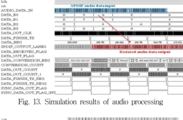
Fig. 13 shows the simulation result of the DisplayPort main link audio data sink block in receiver. Secondary data sink block converts audio data coming from transmitter block to SPDIF format and transmits audio data to audio output ports. Fig. 14 shows the simulation result of merged video and audio for main link. As shown the audio data inserts blanking period of video timing.
Fig. 12. Simulation result of video processing
Fig. 13. Simulation results of audio processing
Fig. 14. Simulation results of video/audio processing Fig. 15 shows link training result of link policy maker in AUX channel receiver. When CRlock, EQdone, SYMBOLlock, and INTERLANE signals are high, the link training state is in normal operation state. The measured result of main link video and audio outputs by using signal tap2 logic analyzer is shown in Fig. 16. The video data consist of RDE, RHS, RVS and RE_RGB. The output data are TDE, THS, TVS and TE_RGB.
Audio input and output signals, AUDIO_DATA_IN and SPDIF_OUTPUT_LANE0 are also shown in bottom of Fig. 16. Fig. 17 shows the testing environment using real data. The audio and video data sources are obtained from a PC and provide them to the designed DisplayPort link layer. The left side is for known data from the PC, and the right side monitor and speaker are used to confirm the video and audio data coming out from the designed DisplayPort link layer.
Fig. 15. Link training result of link policy maker.
Fig. 16. Measured result of main link video and audio outputs by using signal tapⅡ logic analyzer.
Fig. 17. Test environment with real data The merged video/audio link with AUX channel is implemented with 7,648 LUTs(Look Up Tables), 6068 registers, and 821,760 of block memory bits and it is synthesized using a FPGA board and operates at 203.32MHz . The performance summary of the DisplayPort Link Layer is given in Table I.
Table 1. Design summary of displayport link layer DisplayPort Link Layer
Logic utilization
LUTs 7,648
Registers 6,020
Total Block Memory bits 821,760 Maximum Frequency 203.32 MHz
V. CONCLUSION
This paper presents a link layer design of DisplayPort interface with a state machine based on packet processor. The link layer based on state machines is designed to provide extensibility and all data are packetized to facilitate data processing. The verification of the design implemented on a FPGA is confirmed via real data testing. The merged video, audio main link with AUX channel controller was implemented with 7,648 LUTs, 6020 registers, and 821,760 of block memory bits. The design was synthesized using a FPGA board and the board operates at 203.32MHz.
References
[1] VESA, “VESA DisplayPort Standard”, Version 1, Revision 1a, January 11, 2008.
[2] VESA, “DisplayPort Link Layer Compliance Test Standard”, Version 1.0, September 14, 2007.
[3] CEA, A DTV Profile for Uncompressed High Speed Digital Interfaces, CEA-861-C, pp69-74, August 2005.
[4] IEC, Digital Audio Interface – part1 : general, IEC 60958-1, September 2008.
[5] IEC, Digital Audio Interface – part3 : Consumer application, IEC 60958-3, May 2006.
BIOGRAPHY
Hyun-Bae Jin (Student Member) 2009 : BS degree in Electronics Engineering, Inha University.
2009 ~ Present : MS candidate in Electronics Engineering, Inha University.
Kwang-Hee Yoon (Member)
2008 : BS degree in Electronics Engineering, Inha University.
2010 : MS degree in Electronics Engineering, Inha University.
2010 ~ Present : Research Engineer, Silicon Works Co., Ltd.
Tae-Ho Kim (Student Member) 2007 : BS degree in Electronics Engineering, Inha University.
2009 : MS degree in Electronics Engineering, Inha University.
2009 ~ Present : Ph.D.
candidate in Electronics Engineering, Inha University.
Ji-Hoon Jang (Non Member)
2009 : BS degree in Electronics Engineering, Ho-Seo University.
2009 ~ Present : MS candidate in Electronics Engineering, Inha University.
Byung-Cheol Song (Non Member)
1994 : BS degree in Electrical Engineering, Korea Advanced Institute of Science and Technology (KAIST).
1996 : MS degree in Electrical Engineering, Korea Advanced Institute of Science and Technology (KAIST).
2001 : PhD degree in Electrical Engineering, Korea Advanced Institute of Science and Technology (KAIST).
2001 ~ 2008 : Senior engineer, Samsung Electronics Co., Ltd.
2008 ~ Present : Assistant professor, Inha University.
Jin-Ku Kang (Member)
1983 : BS degree in Nuclear Engineering, Seoul National University.
1990 : MS degree in Electrical and Computer Engineering, New Jersey Institute of Technology.
1996 : PhD degree in Electrical and Computer Engineering, North Carolina State University.
1984 ~ 1988 : Research engineer, Samsung Electronics Co., Ltd.
1988 : Research engineer, Texas Instrument Korea.
1996 ~ 1997 : Senior design engineer, Intel(U.S).
1997 ~ Present : Professor, Inha University.