*준회원, 전북대학교 IT응용시스템공학과
**정회원, 전북대학교 IT응용시스템공학과(교신저자)
***정회원, 전북대학교 IT응용시스템공학과
****정회원, 전북대학교 IT응용시스템공학과
접수일자 : 2015년 9월 24일, 수정완료 2015년 10월 7일 게재확정일자 : 2015년 10월 9일
Received: 24 September, 2015 / Revised: 7 September, 2015 / Accepted: 9 October, 2015
**Corresponding Author: [email protected]
Dept. of IT Applied System Engineering, Chonbuk National University, Korea
http://dx.doi.org/10.7236/JIIBC.2015.15.5.201
JIIBC 2015-5-25
OTA기반의 차단대역 조정이 가능한 3-입력/1-출력 구조의 다기능 Gm-C 필터
Stopband Tunable Multifunctional Gm-C Filter based on OTA with Three-Input/Single-Output
바스넷버룬*, 방준호**, 송제호***, 유인호****
Barun Basnet*, Jun-Ho Bang**, Je-ho Song***, In-Ho Ryu****
요 약 본 논문에서는 연산 트랜스컨덕턴스 증폭기를 기반으로 하여 차단주파수 대역의 조정이 가능한 3-입력와 1- 출력단을 갖는 Gm-C필터가 제안되었다. 제안된 필터는 대역통과, 저역통과 및 고역통과의 다기능 필터 특성을 갖는다.
구현된 필터의 중심주파수()와 특성요소(Q)값은 다른 필터특성의 변형없이 독립적으로 조정이 가능할 수 있음을 확 인하였다. 또한 전체 시스템에 영향을 줄 수 있는 다양한 파라미터들과 기생요소들에 대한 감도특성과 비이상성분석이 수행되었다. 제안된 필터를 CMOS 소자로 구현하기 위하여 1.8V-0.18um 공정파라미터를 사용하였고 HSPICE를 활용 하여 특성을 분석한 결과와 기 정리된 이론값들과 비교하여 나타내었다.
Abstract A new electronically stopband tunable filter is proposed with three-input single-output using Operational Transconductance Amplifier (OTA) in this paper. The proposed filter provides band pass, low pass and high pass multifunctional responses. Centre frequency () and quality factor (Q) of the realized filters could independently tuned without disturbing each other. Various network sensitivity and non-ideal characteristic analysis are done to check the sensitivity and parasitic effect of different circuit parameters. The CMOS realization of filter is done with 1.8V-0.18um process parameters and HSPICE simulation results are presented to assert the presented theory.
Key Words : OTA, Multifunctional filter, Transconductance, Gm-C, Bandpass
Ⅰ. Introduction
The evolution of the wireless and low voltage devices has led Operational Transconductance Amplifiers (OTA) to appear in the field of analog integrated circuit design[1]-[4]. Unlike Op-Amps which have input stage, gain stage and output stage OTAs
have only input stage and gain stage. With no output stage, the OTA is more compact and consumes less power and have overall output resistance of a large value. The gain stage in OTA produces a current output rather than a voltage which is transconductance (). The single stage gain of OTA further simplifies the internal design, resulting in a simple, fast, compact
amplifier which proves to be efficient in high-frequency and low voltage applications allowing very advanced filters to be implemented on a single silicon chip[5]-[6].
Filters can be classified as single input multiple output (SIMO) or multiple input single output (MISO) type depending upon the number of input and output ports[7]-[10]. Unlike SIMO, the MISO configuration can realize multifunction outputs by altering the way in which the input signals are connected. Also they provide a variety of circuit characteristics with different input voltage and usually does not require any parameter matching conditions. Therefore to realize a larger variety of filter functions MISO configuration seems to be more desirable[11]-[12]. Proposed filter is a multifunctional voltage mode biquadratic filter with three input single output. The proposed filter exhibits low circuit parameters sensitivity and orthogonal tuning capabilities of and Q. The proposed filter uses minimum number of active () and other passive (C) elements [Table 1]. The circuit is simulated in HSPICE using Metal Oxide Semiconductor Implementation Service (MOSIS) 1.8V-0.18 µm SPICE datasheet process parameters.
Ⅱ. Operational Transconductance Amplifier (OTA)
OTA circuits are extensively used in active filters design. An ideal OTA is a voltage controlled current source (VCCS). It uses it inverting and non-inverting voltage inputs to give current output with the externally controlled transconductance () gain as shown in Figure 1.
(a)
(b)
Fig. 1. (a) Block diagram of OTA (b) Small Signal Equivalent Circuit of OTA
그림 1. (a) OTA 블록다이어그램 (b) OTA 소신호 등가 회로
Fig. 1(a) represent block diagram of OTA and Fig.
1(b) represents small signal equivalent circuit of OTA.
(1)
Here, is the output current and is the transconductance gain and and are inverting and non-inverting voltage inputs respectively.
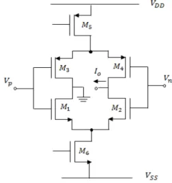
Fig. 2. CMOS implementation of OTA 그림 2. CMOS로 구현된 OTA
Assuming four MOS transistors operating in saturation regions, the value can be expressed as equation (2).
(2)
where is the bias current, is the effective carrier mobility, is the gate-oxide capacitance per unit area, and W/L is the ratio of effective channel width and length of an individual MOS transistor.
Ⅲ. Design of a Multifunctional Filter
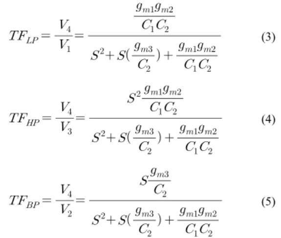
A second order multifunctional filter with 5 MHz is realized using three OTAs and two capacitors as shown in Figure 3. OTA-based filters are referred to as Gm-C filters because they use OTAs and capacitors.
Here, Fig. 3 is the designed second order Gm-C filter which can realize low pass (LP), high pass (HP) filter and band pass (BP). If and are taken as input and output respectively while assigning and , the LP filter transfer function can be realized as in the equation (3). Similarly, if and are taken as input and output respectively while assigning and the HP filter transfer function can be realized as in the equation (4). Lastly, if and are taken as input and output respectively while assigning and the BP filter transfer function can be realized as in the equation (5).
Fig. 3. The designed second order multifunctional Gm-C filter
그림 3. 설계된 2차 다기능 Gm-C Filter
(3)
(4)
(5)
The angular frequency () and Q factor of the multifunctional filter can be derived as in equation (6) and (7) respectively.
(6)
(7)
If all the other transconductances are kept constant and only is adjusted separately then a controllable value for Q factor can be derived.
Also, if every transconductance gain are assigned equal value i.e , then we have center frequency as shown in equation (8).
(8)
Hence, the realized band pass filter circuit can independently control and Q factor. The sensitivity analysis of the proposed multifunctional filter can be derived as in equation (9).
,
(9)
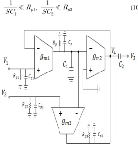
The effect of parasitic elements are also considered to have a non-ideal circuit analysis of the multifunctional filter as shown in Figure 4.
Here , , and are parasitic resistances
whereas , , and are parasitic capacitances in the filter . Generally value of and
are in excess of the expected parasitic capacitances, these parasitic capacitances can be absorbed at working frequencies. However to minimize the parasitic resistances following condition must be fulfilled as shown in equation (10).
≪,
≪ (10)
Fig. 4. Parasitic impedance of Gm-C filter 그림 4. Gm-C 필터의 기생 임피던스
The following table compares the number of passive and active elements used in realizing a second order filter with other papers published so far.
References
Number of Passive and active Elements used
R C
[6] 6 3 0
[7] 6 0 2
[8] 4 2 3
[9] 4 0 2
Proposed 3 0 2
Table 1. Comparison of Proposed Filter with other references
표 1. 다른 필터 구조와의 비교
As seen in the Table 1. reference [6] and [7] has used six transconductances with three resistors and two capacitors respectively. Reference [8] has only
used four transconductances but it has included two resistors and three cpapacitors. Reference [9] has used four transconductances with only two capacitors eliminating resistors. The proposed method only uses three transconductances and two capacitors for constructing a biquad filter.
Ⅳ. Simulation Results
The internal structure of the OTA (Fig.2) was simulated using MOSIS 0.18µm CMOS process model parameters with DC supply voltage of 1.8 V. All the parameter values were assigned to pull 400µA tail current. Aspect ratio (W/L) of all current biasing PMOS and NMOS transistors were taken as 15.6 and 3.44 respectively. And value of 38.22 and 52.27 was taken for all remaining NMOS and all PMOS transistors respectively. Active component values were selected as = 31.428µS. In the case of the simulated multifunctional filter, both and were assigned with the value of 1 pF.
Fig. 5. Frequency response of the designed multifunctional filter
그림 5. 설계된 다기능 필터의 주파수 응답
Here, Fig. 5 represents simulated frequency response of LP, BP and HP filter with 5 MHz center frequency.
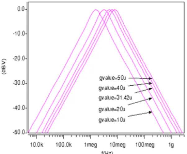
Fig. 6 and 7 represents tuning of from 1.5 MHz to
10 MHz and Q factor from 3.1 to 0.62 when value is changed from 10 µS to 50 µS. Thus the simulation result confirms the presented theory.
Fig. 6. Tuning of the designed BP filter 그림 6. 설계된 BP 필터의 조정특성
Fig. 7. Tuning Q factor of the designed BP filter 그림 7. 설계딘 BP 필터의 Q값 조정특성
Ⅴ. Conclusion
This paper presents design of a voltage mode biquadratic Gm-c filter with three input one output. It only employs three OTAs and two capacitors for realizing a multifunctional filter frequency responses.
This circuit offers electronically tunable capability of
and Q factor without disturbing each other. Parasitic element analysis were also done as non-ideal analysis and HSPICE simulation results were presented using MOSIS 0.18 µm process parameters as a functional verification. The proposed multifunctional Gm-C filter will be applied for designing small size and low power analog circuits.
References
[1] Myung-Sik Shin and Hae-sool Yang, ‘Performance of Turbo Coded OFDM Systems in W-CDMA Wireless Communication Channell’, The Journal of The Institute of Internet, Broadcasting and Communication (JIIBC), Vol. 10 No.4, Aug 2010 [2] Jyotirmoy Ghosh, Insoo Koo, ‘An Approach to
Maximize throughput for Energy Efficient Cognitive Radio Networks’, International Journal of Advanced Culture Technology IJACT, Vol.1, No.2, 2014 [3] Songwon Kim, ‘Design and Fabrication of the
GPS Receiving Antenna using Hilbert Curve Fractal Structure’, Journal of The Institute of Internet, Broadcasting and Communication JIIBC, Vol.14, No.1, 2014.
[4] Seongsoo Cho, Bhanu Sherstha et al., ‘Energy Efficient Routing in Wireless Sensor Networks’, International Journal of Advanced Smart Convergence IJASC, Vol.3, No.2, 2014
[5] Nong Jun, Kee Hyon et al., ‘RFID-based Secure Communication for Smart Device in Future Home Network Environment’, Int. Journal of Internet, Broadcasting and Comm. IJIBC, Vol.5, No.1, pp 14-17, 2014.
[6] Kim Jinyoung, Jung Changwon, ‘Broad Band Stop Filter Using Frequency Selective Surface Embeded in Microwave Transmission Line’, Journal of the Korea Academia-Industrial Cooperation Society, Vol.13, No.12, 6022-6026, Dec 2012
[7] Montree Kumngern and Kobchai Dejhan, ‘Electronically
Tunable Voltage-Mode Universal Filter with Three-Input Single-Output’, International Conference on Electronic Devices, System and Applications (ICEDSA), IEEE, 2010
[8] R. Senai and D. R Bhaskar, “New lossy/loss-less synthetic floating inductance configuration realized with only two CFOAs”, Springer, Analog Integrated Circuits and Signal Processing, pp. 981 –987. 2012
[9] Jetsdaporn satansup, Worapong Tangsrirat, ‘Compact VDTA-based current-mode electronically tunable universal filters using grounded capacitors’, Microelectronics Journal 45(2014) 613-618 [10] W.T Lee and Y.Z Liao, ‘New Voltage-mode
high-pass, band-pass and low-pass filter using DDCC and OTAs’, International Journal of Electronics and Communications, Vol.62, pp 701-704, 2008 [11] A.F Arbel, L.Goldminz, ‘Output stage for
current-mode feedback amplifiers, theory and applications’, Analog Integr.Circ.Sig.Process 2(3), 243-255, 1992
[12] Trung-Kien Nguyen, ‘A Low Voltage Low Power CMOS Fifth Order Elliptic Low Pass Gm-C Filter For Direct Conversion Receiver’, Asia-Pacific Microwave Conference, 2003
저자 소개
바스넷버룬(준회원)
∙2014년 ∼ 현재 : 전북대학교 IT응용시 스템공학과 석사과정
<주관심분야 : 아날로그 회로설계, IT융 합시스템회로 설계>
방 준 호(정회원)
∙1996년 : 전북대학교 전기공학과 박사
∙1997년 ∼ 1998년 : LG반도체 기술연 구소 선임연구원
∙1998년∼ 현재 : 전북대학교 IT응용시 스템공학과 교수
<주관심분야 : 아날로그 회로설계, IT융 합시스템회로 설계>
송 제 호(정회원)
∙2003년 : 원광대학교 전자공학과 박사
∙1996년 ∼ 현재 : 전북대학교 IT응용시 스템공학과 교수
<주관심분야 : IT융합, 통신 네트워크 시 스템 설계, DSP설계>
유 인 호(정회원)
∙1999년 : 원광대학교 전기공학과 박사
∙1993년∼ 현재 : 전북대학교 IT응용시 스템공학과 교수
<주관심분야 : 자동제어, 스마트그리드 전기 시스템 설계>