High-Resolution X-Ray Photoelectron Spectroscopy Study of a Sb
2Te
3Thin Film with the Polycrystalline Phase
Y. M. Leea, K. Kimb, H.-J. Shinc, M.-C. Jungd*, and Y. Qid†
aDepartment of Materials Engineering, Chungnam University, Brain Korea 21 Project (BK21), Daejeon 305-764
bAE Group, Samsung Advanced Institute of Technology, Samsung Electornics Co. Ltd., Yongin 446-711
cBeamline Division, Pohang Accelerator Laboratory, POSTECH, Pohang 790-784
dEnergy Materials and Surface Sciences Unit, Okinawa Institute of Science and Technology Graduate University, Okinawa, Japan 904-0495
(Received September 28, 2012, Revised November 21, 2012, Accepted November 22, 2012)
We investigated chemical states of a Sb2Te3 thin film with the polycrystalline phase by using high-resolution x-ray photoelectron spectroscopy with synchrotron radiation. The Sb2Te3 thin film was formed by sputtering. The rhombohedral phase was confirmed by x-ray diffraction. To remove the surface oxide, we performed Ne+ ion sputtering for 1 hour with the beam energy of 1 kV and post-annealing at 100oC for 5 min in ultra-high vacuum. We obtained the Te and Sb 4d core-levels spectra with the peaks at the binding energies of 40.4 and 33.0 eV, respectively. The full-width of half maximum of both the Te and Sb 4d5/2 core-levels is 0.9 eV. The Te and Sb core-levels only show a single chemical state, and we also confirmed the stoichiometry of approximately 2:3.
Keywords : Sb2Te3, Chemical state, High-resolution x-ray photoelectron spectroscopy
I. Introduction
Chalcogenide phase-change materials have been attracting much attention as promising materials for non-volatile memories such as phase-change random access memory (PRAM) because of the reversible change in the electrical properties between amorphous and crystalline phases [1]. Among the chalcogenide materials, the GeTe-Sb2Te3 pseudo-binary films have been widely investigated as a candidate for the re- writable optical disk and PRAM applications [1-4].
In particular, the binary compound Sb2Te3 shows very high crystallization speed and low reset power be- cause of its relatively low melting point. Although the
low crystallization temperature (<100oC) prevents its practical application in PRAM, doping with other ele- ments is under scrutiny to improve the stability of the amorphous phase [3,4]. Many research groups have fo- cused on device fabrication, rapid crystallization, and enhanced phase stability for PRAM application. To support PRAM applications, we need to obtain and un- derstand atomic and electronic structures of phase- change materials. However, the chemical states of phase-change materials has not been fully investigated systematically. And it is also very difficult to obtain exact chemical states of phase-change materials be- cause these materials have rapidly an oxide con- tamination with the thickness of 20 nm to exposure on
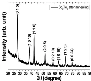
Figure 1. XRD diffraction pattern of Sb2Te3 thin film was performed by the post-annealing for 5 min in UHV after Ne+ mild sputtering for 1 hour with the beam energy of 1 kV.
the air [5-9]. Normally, we perform an Ar+ ion sput- tering in ultra-high vacuum to remove surface con- tamination [10]. However, it is difficult to remove the surface oxide with the fitted stoichiometric surface in these phase-change materials [11]. In this PRAM re- search, it is needed to find a good surface treatment method [12,13].
In the present study, we examined amorphous and polycrystalline phase of Sb2Te3 by high-resolution x-ray photoelectron spectroscopy (HRXPS) with syn- chrotron radiation. Clean oxygen-free amorphous Sb2Te3 was obtained by Ne+ sputtering to remove the surface oxide and obtain the 2:3 stoichiometric sur- face, and crystallization was performed by resistive heating at 100oC for 5 min under ultra-high vacuum (UHV). The differences between the chemical states prior to and after crystallization were investigated.
II. Experimental Procedure
The Sb2Te3 thin film was deposited by radio-fre- quency magnetron sputtering on a Si wafer at room temperature. We used a Sb2Te3 single target and Ar gas. The base and working pressures are 1.2×10⁻⁶ and 1.5×10⁻³ Torr, respectively. The thickness of the deposited Sb2Te3 thin film is 100 nm determined by quartz crystal microbalance. The structural phase, total thickness (100 nm), and the native oxide thick- ness (20 nm) of the sample were confirmed by x-ray diffraction (XRD) and secondary ion mass spectro- scopy (SIMS). To remove the oxide layer formed on the surface of the thin film sample when exposed to air, the Sb2Te3 sample was sputtered by Ne+ (99.999%) for 1 hour with the ion-beam energy of 1 kV under the pressure of 1.0×10⁻⁵ Torr [5-9]. The sputtering time was long enough to remove all 20 nm thick oxi- dized layers. For comparison, spectral data obtained after 30 min sputtering time are provided, where a strong oxygen trace is observed near Sb 3d spectrum
(Fig. 2(a)). After ion sputtering for 1 h no trace of O 1s peak was observed and the Sb and Te spectral in- tensities represented the desired stoichiometry. To crystallize Sb2Te3, the oxygen-free Sb2Te3 thin film was annealed by resistive heating for 5 min at 100oC under the pressure of 5.0×10⁻¹⁰ Torr. Also, the chemical states of the obtained Sb2Te3 were inves- tigated by HRXPS using the Pohang Light Source (PLS) synchrotron at beamline 8A1 (U7) [14]. The in- cident photon energy was 250 eV. A PHI 3,057 with an Omega lens and a 16-channel detector (Physical Electronic Co.) was used as the electron analyzer.
The energy resolution was better than 200 meV. The core-level spectra of the Te and Sb 4d were also obtained. The binding energies were calibrated with reference to the Au 4f 7/2 level (84.0eV) [15].
III. Result and Discussion
Fig. 1 showed the XRD diffraction pattern of Sb2Te3
which was sputtered with the Ne+ ions with the beam energy of 1 kV for 1 hour followed by post-annealing
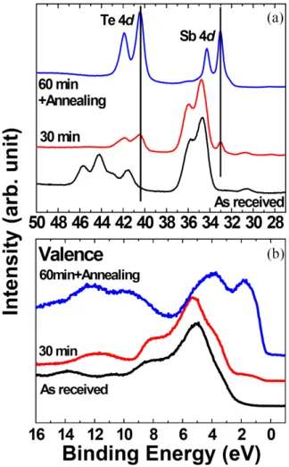
Figure 2. (a) Te and Sb 4d core-levels and (b) valence spectra of the as-received, the sputtering for 30 min and the post-annealing for 5 min after sputtering for 60 min. The last spectrum of core-level and valence was shown with the only chemical states of Sb2Te3 without the impurities.
for 5 min in UHV. We confirmed that these peaks can be attributed to the rhombohedral phase, which is consistent with the previous observations [16,17].
Fig. 2 shows the Te, Sb 4d core-levels and valence spectra. The core-level spectra of the as-received, after sputtering for 30 min, and after 60 min sput- tering followed by post-annealing for 5 min are shown in Fig. 2(a), respectively. In the as-received sample, the peak positions of the Sb-Te oxide are at 44.2, 41.5 and 34.7 eV of Te and Sb 4d5/2 core- levels, respectively. We assumed that chemical states of two Te oxides were originated from Te-O and
Te-O-Sb included with Sb oxide, respectively [12,13].
These peak position values are close to Ge2Sb2Te5
with oxide on the surface [10]. After mild Ne+ sput- tering for 30 min, the Te oxide core-level peaks at 44.2 and 41.5 eV disappeared while a new peak ap- peared at 40.4 eV. Also, the Sb-oxide core-level peak at 34.7 eV still remained. We assume that the sputtering ratios of Te and Sb by Ne+ ion sputtering are different and also it was observed in Ge2Sb2Te5
thin film of our old study [6,11]. However, we can notice the new peak at 33.0 eV for Sb 4d5/2 core- level. After sputtering for 60 min followed by post- annealing for 5min in UHV, we can observe clearly the single chemical states of Te and Sb 4d core-levels at 40.4 and 33.0 eV, respectively. We assumed that these peaks were represented in their own stoi- chiometry without any oxygen components [6]. The relative oxide peaks completely disappeared and the peak shape was much sharper. The Te and Sb 4d core-levels were enhanced with the large intensities and fine shapes. The full-with of half-maximum (FWHM) of both Te and Sb 4d5/2 core-level peaks were measured to be 0.9 eV.
In Fig. 2(b), the valence spectra of the as-received and after sputtering for 30 min samples were shown with typical oxide. Such a valence spectrum (at the binding energies of ∼5, ∼8.5, and ∼14 eV in the figure) showed a similar shape with that of the Ge-Sb-Te alloy materials [7-9]. We can observe the peaks that correspond to the chemical states of Te 5s, Sb 5s and their hybridization. After sputtering for 60 min followed by post-annealing for 5 min in UHV, we can also observe the Fermi-edge. It means that the oxide on the surface is completely removed and it has a metallic property. We assumed that the Te 5p and Sb 5p orbitals in the binding energy range of 0∼6 eV is mostly similar to the peak shapes reported by Klein, et al [18,19]. We considered in these results that there were consistent to our core-level interpretations.
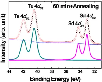
Figure 3. Curve fitting data of Te and Sb 4d core-levels in Sb2Te3 thin film was performed by the post-annealing for 5 min in UHV after Ne+ sputtering for 60 min.
In order to analyze the spectrum in detail, curve fitting was performed to the Te and Sb 4d core-level spectra using convoluted Doniach-Sŭnjić curves, which is shown in Fig. 3 [20]. The background noise due to inelastic scattering was subtracted using the Shirley (or integral) method [21]. The Te and Sb 4d core-level spectra illustrated the spin-orbit splitting with the branching ratio of 2:3 for d orbital at 1.5 and 1.2 eV, respectively [15]. The curve-fitting re- sults were performed by using only a single chemical state for both Te and Sb 4d core-levels.
The atomic percent of the elements was estimated from the curve-fittings in Fig. 3, with the reported values of the atomic sensitivity factor (ASF) and the atomic subshell photoionization cross section (ASPCS) [22]. The relative ASF and ASPCS values at 250 eV photon energy are 1.00:1.23 and 0.7476:0.7741 for Sb 4d:Te 4d, respectively. The measured area ratio is 0.9488:1.5432 and the estimated atomic percent ratio is approximately 18:32 for Sb:Te, confirming the preservation of stoichiometry. A little less of Sb concentration is likely due to the surface depletion of Sb atom by the short post-annealing.
IV. Conclusions
We performed the HRXPS measurement with syn- chrotron radiation on a Sb2Te3 thin film with the pol- ycrystalline phase. To remove the surface oxide on the surface of the Sb2Te3 thin film sample, we performed the Ne+ mild ion sputtering with the beam energy of 1 kV. The sample was subsequently annealed at 100oC for 5 min in UHV. In this sample, we obtained the chemical states of Te and Sb 4d core-level in the oxy- gen-free Sb2Te3 at the binding energies of 40.4 and 33.0 eV, respectively. This process restored the origi- nal chemical states of Sb2Te3 without the oxygen im- purity while preserving stoichiometry.
Acknowledgments
M.-C.J. and Y. Qi would like to acknowledge the internal funding from Okinawa Institute of Science and Technology Graduate University in Japan. Y.M.L.
would like to acknowledge the financial support of the Brain Korea 21 Project funded by the Korean Government.
References
[1] N. Yamada, E. Ohno, K. Nishiuchi, N. Akahira, and M. Takao, J. Appl. Phys. 69, 2849 (1991).
[2] A. V. Kolobov, P. Fons, A. I. F Renkel, A. L.
Ankudinov, J. Tominaga, and T. Uruga, Nat. Mat.
3, 703 (2004).
[3] Y. Yin, H. Sone, and S. Hosaka, J. Appl. Phys.
102, 064503 (2007).
[4] M. S. Kim, S. H. Cho, S. K. Hong, J. S. Roh, and D. J. Choi, Ceramics International 34, 1043 (2008).
[5] M.-C. Jung, H. J. Shin, K. Kim, J. S. Noh, and J. Chung, Appl. Phys. Lett. 89, 043503 (2006).
[6] M.-C. Jung, H. J. Shin, K. Kim, J. S. Noh, and
J. Chung, Appl. Phys. Lett. 89, 043503 (2006).
[7] M.-C. Jung, K. Kim, Y. M. Lee, J.-H. Eom, J. Im, Y.-G. Yoon, J. Ihm, S. A. Song, H. S. Jeong, and H.-J. Shin, J. Appl. Phys. 104, 074911 (2008).
[8] M.-C. Jung, Y. M. Lee, K. Kim, J. C. Park, S. A.
Song, H.-D. Kim, H. S. Jeong, and H. J. Shin, Curr.
Appl. Phys. 10, 1336 (2010).
[9] Y. M. Lee, Y. Park, C.-W. Sun, J. Y. Lee, H. J.
Shin, Y. T. Kim, and M.-C. Jung, Thin Solid Films 518, 4442 (2010).
[10] K.-H. Park, S.-K. Cho, and T.-U. Nahm, J. Korean Vac. Soc. 17, 183 (2008).
[11] S.-P Kim, S.-J Kim, D.-Y. Kim, Y.-C. Chung, and K.-R. Lee, J. Korean Vac. Soc. 17, 81 (2008).
[12] J. H. Oh, S. W. Ryu, B. J. Choi, S. Choi, C. S.
Hwang, H. J. Kim, S. Y. Hwang, Y. J. Kim, H.
C. Park, H. Y. Chang, and S. K. Hong, J. Korean Phys. Soc. 49, 1173 (2006).
[13] M.-Y Kim, K.-W Park, and T.-S. Oh, J. Korean Phys. Soc. 53, 266 (2006).
[14] M. K. Lee and H. J. Shin, Rev. Sci. Instrum. 72,
2065 (2001).
[15] J. F. Moulder, W. F. Stickle, P. E. Sobol, and K.
D. Bomben, Handbook of X-ray Photoelectron Spectroscopy (Physical Electronics, Eden Prairie, MN, 1995), p. 93.
[16] X. Lia, F. Rao, Z. Song, K. Ren, W. Liu, and Z.
Sun, Appl. Sur. Sci. 257, 4566 (2011).
[17] B. Yu. Yavorsky, N. F. Hinsche, I. Mertig, and P.
Zahn, Phys. Rev. B 84, 165208 (2011).
[18] A. Klein, H. Dieker, B. Spaeth, P. Fons, A.
Kolobov, C. Steimer, and M. Wuttig, Phys. Rev.
Lett. 100, 016402 (2008).
[19] J.-J. Kim, K. Kobayashi, E. Ikenaga, M. Kobata, S. Ueda, T. Matsunaga, K. Kifune, R. Kojima, and N. Yamada, Phys. Rev. B 76, 115124 (2007).
[20] S. Doniach and M. Sŭnjić, J. Phys. C 3, 285 (1970).
[21] D. A. Shirley, Phys. Rev. B 5, 4709 (1972).
[22] D. Briggs and M. P. Seah, Auger and X-ray photoelectron spectroscopy practical surface analysis Vol. 1, 1st ed. (Wiley, NewYork, 1990).
고해상도 엑스선 광전자 분광법을 이용한 다결정구조의 안티몬-테레니움 박막 연구
이영미aㆍ김기홍bㆍ신현준cㆍ정민철d*ㆍ취야빙d†
a충남 대학교 재료공학부 BK21, 대전 305-704
b삼성전자 삼성종합기술원 AE 그룹, 용인 446-711
c포스텍 포항가속기연구소 빔라인부, 포항 790-784
d오키나와 과학기술대학원 대학 에너지 물질 및 표면 과학 그룹, 오키나와, 일본 904-0495
(2012년 9월 28일 받음, 2012년 11월 21일 수정, 2012년 11월 22일 확정)
스퍼터를 이용하여 실리콘 기판위에 제작된 안티몬-테레니움 다결정 박막을 방사광을 이용한 고해상도 엑스선 광전자 분광법 실험을 수행하여 화학적 상태를 분석하였다. 엑스선 회절 실험을 통해 제작된 안티몬-테레니움 박막은 롬보헤드럴 구조를 가지 는 다결정임을 확인하였다. 엑스선 광전자분광법을 수행하기 위하여 표면의 산화막 제거를 위해 저에너지 네온 이온 스퍼터링 을 빔에너지 1 kV로 1 시간동안 수행하였고, 이를 통해 표면 산화막이 완벽히 제거됨을 확인하였다. 또한, 스퍼처링에 의하여 표면 비정질화된 상태를 결정화 상태로 만들기 위해 상변화온도인 100oC에서 5 분간 초고진공상태에서 열처리를 수행하였다.
이후 획득되어진 테레니움 4d와 안티몬 4d 속전자레벨 분석에서 각각의 묶음에너지가 40.4 그리고 33.0 전자볼트임을 확인할 수 있었으며, 각각은 단일한 화학적 상태를 나타내고 얻어진 피크의 밀도분석을 통해 화학적조성비가 2:3임을 확인하였다.
주제어 : 안티몬-테레니움 박막, 화학적 상태 분석, 고해상도 엑스선 광전자분광법
* [전자우편] [email protected]
† [전자우편] [email protected]