碩士學位論文
대면적, 고화질 TFT-LCD 적용을 위한 저저항 Ag-alloy 배선 공정 연구
A study on low resistivity Ag-alloy metallization for application to large-area and high resolution TFT-LCD
國民大學校 大學院 金屬材料工學科
姜 奉 周
2001
碩士學位論文
대면적, 고화질 TFT-LCD 적용을 위한 저저항 Ag-alloy 배선 공정 연구
A study on low resistivity Ag-alloy metallization for application to large-area and high resolution TFT-LCD
指導敎授 李 在 甲
이 논문을 석사학위 請 求 論 文 으 로 提出함
2001年 12月
國民大學校 大學院 金屬材料工學科
姜 奉 周
2001
姜 奉 周 의
碩 士 學 位 請 求 論 文 을 認准함
2001年 12月
審 査 委 員 長 印 審 査 委 員 印 審 査 委 員 印
國民大學校 大學院
Abstract
The effect of Mg in Ag(Mg)/SiO2/Si multilayers on adhesion, agglomeration, and resistivity after annealing in a vacuum at 200℃ to 500℃ have been investigated. The annealing of Ag(Mg)/SiO2/Si multilayers produced surface and interfacial MgO layers, resulting in MgO/Ag(Mg)/MgO/SiO2/Si structure. The presence of surface MgO provided the passivation against air, thus leading to the significantly enhanced resistance to agglomeration. In addition, Ag adhesion to SiO2 was improved due to the formation of the interfacial MgO layer resulting from the reaction of Mg with SiO2. However, the interfacial reaction proceeded to a limited extent. Ag has a negligible solubility of free silicon, which limits the interfacial MgO formation. As a result, the resistivity of Ag(10 at.% Mg) continued to decrease with annealing temperature and became 2.9 μΩ-cm after annealing at 500℃.
List of Figures
Fig. 1. Mg behavior in Ag(Mg) alloy during annealing
Fig. 2. Resistivity variation of Ti(70Å)/Ag/Si with annealing temperature in vacuum.
Fig. 3. AES depth profiles of Ti(70Å)/Ag(2000Å)/Si annealed at various temp (a)as-dep, (b)500℃, and (c)700℃.
Fig. 4. Resistivity variation of Ag(Mg) alloy with annealing temperature and Mg concentration.
Fig. 5. Auger Depth profiles of Ag(10at.%Mg) films/SiO2 annealed in vacuum for 30min (a) as-dep, (b) 300℃, (c) 400℃, and (d) 500℃.
Fig. 6. Resistivity variation of Ag(10at.%Mg)alloy films annealed for 1.0 to 60min at 400℃ and 500℃, respectively.
Fig. 7. AES depth profiles of Cu(4.5 at.% Mg)/SiO2/Si multilayers annealed in 10 mTorr of O2 for various annealing times; (a) 1 min, (b) 3 min, (c) 10 min, and (d) 90 min.
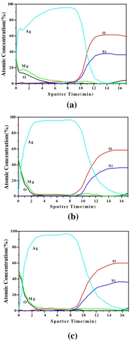
Fig. 8. AES depth profile of Ag(10at.%Mg)/SiO2/Si (a)as-deposited and then annealed at 400℃ for (b)3min and (c)60min, respectively.
Fig. 9 Stress variation of (a)pure Ag, (b)Ag(10at.%Mg) with annealing temperature.
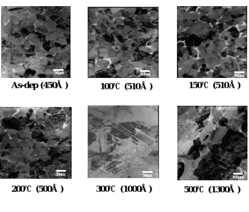
Fig. 10. Plan-view TEM of Ag(10at.%Mg)/TiN/Si annealed in vacuum.
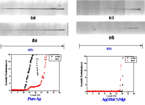
Fig. 11. Scratch images of pure Ag, Ag(10at.%Mg)/SiO2 with annealing.
(a) as-dep of pure Ag, (b) pure Ag annealed at 300℃, (c)
Ag(10at.%Mg), (d) Ag(10at.%Mg) annealed at 300℃.
Fig. 12. Acoustic emission of (a) pure Ag, (b) Ag(10at.%Mg) on O2 plasma treated Si.
Fig. 13. Cross-sectional TEM images of Ag(10at.%Mg) on O2 plasma treatment Si.
Fig. 14. SEM micrograph of pure Ag on SiO2 annealed in air.
Fig. 15 Variation of hole area formed on Ag films deposited on SiO2 upon annealing at 300℃ for various times.
Fig. 16. Sheet resistance variation of a 1000Å-thick and Ag(Mg)/SiO2 annealed in vacuum at 300℃ as a function of annealing temp.
Contents
ABSTRACT………ⅰ LIST OF FIGURES……… ⅱ
1. INTRODUCTION ……… 1
2. BACKGROUNDS ……… 4
2.1. Diffusion doping of silver thin films ……… 4
3. Experimental ……… 8
4. Results ……… 10
4.1. Resistivity ……… 10
4.2. Thermal Stress ……… 21
4.3. Adhesion………27
4.4. O2 plasma treatment………29
4.5. Agglomeration………33
5. Conclusions………39
6 . Reference………40
iv
1. Introduction
Due to the increased use of portable computers (PCs), the market for
active-matrix liquid-crystal-displays (AM-LCDs), which use amorphous
silicon thin film transistor (a-Si TFT) arrays, is growing very rapidly.[1] In
addition, the markets of large TFT-LCDs , as used in LCD-TVs, are also
expanding. However, several fundamental scaling problems are
encountered in attempting to increase the display size.[2] One problem is
associated with gate metallization of the inverted-staggered thin-film
transistors of the active matrix.[3] At the present time, refractory metals
such as tantalum/molybdenum(Ta/Mo), chromium(Cr),[4] and α-
tantalum(α-Ta)[ 5] are used, to ensure stable contacts during TFT
fabrication. The resistivities of these materials are greater than 20 µΩ-cm,
which makes them too resistive to be used in large-area, high-pixel-
density displays .[1] To meet requirements in terms of enlarging the size
of the TFT-LCD panel and simplification using new, low-resistivity
materials must be achieved.[6] Recently, Ag has received attentions as a
potential interconnection in ultra-large scale integration(ULSI) [7,8] and
large area TFT/ LCDs[9] because it shows the lowest resistivity among
metals, high electromigration resistance[10], and high thermal
conductivity[11]. In addition, no diffusion barrier is required to prevent
reaction between Ag and Si in Ag/Si contact structures [9] because Ag is
thermodynamically stable with Si and also has negligible solubility of Si.
If high-quality multilayers are to be grown on oxidized Si and the microstructure of the multilayer are to be correlated to the stress or strain levels and the relaxation are to be correlated to the microstructural changes at elevated temperature, it is crucial to study the behavior of the films during post deposition annealing. A number of approaches to encapsulate the exposed surface of silver have been investigated, including nitridation of Ag-Ti alloy [12] and formation of an aluminum oxynitride diffusion barrier for Ag metallization [12, 13]. Moreover, the addition of another metal layer (e.g., Ti or Cr with Ag, Ti, and Al [14, 15], or Mg with Cu metallization [16-18,19]), has also been explored. In this work, Ag and Ag-alloy films, have been investigated to overcome routine problems including poor adhesion to dielectrics, agglomeration[5] upon annealing in
an oxygen ambient, Ag sulfidation (chlorination) in the corrosive environment[20], and difficulty with dry etching[1]. Among those issues, this work will be focused on two crucial problems such as poor adhesion to SiO2 and agglomeration using an Ag(Mg) alloying scheme. The doping of Ag with Mg was intended to grow the surface MgO layer to passivate the Ag and to produce the interfacial MgO layer on SiO2 surface upon annealing. The formation mechanism of surface MgO and interfacial MgO layer will be described. Furthermore, the factors affecting the interfacial MgO reaction, its effects on the adhesion and the resistivity of Ag(Mg) alloy films will be discussed.
2. Background
2.1. Diffusion doping of silver thin films
A passivation by the formation of a barrier layer of metal oxide is a common mechanism for the passivation of metals. It is the mechanism responsible for the passivation of Al, which is chemically a very reactive metal. And it is the fact that Ag is not an effective barrier layer that leads to the poor oxidation resistance of pure Ag. The fact that this inert surface oxide is formed as a result of a reaction between the dopant metal and impurities in the annealing ambient suggests that optimizing this process will require more careful study of how this oxide is formed. It is also interesting to note that magnesium which does not always form a self- passivating oxide on the surface of Mg metal. There are indications that the dopant metals are also being oxidized at the interface with the SiO2 substrate. This reaction leads to much improved adhesion of the metal to the substrate and possibly forming a barrier oxide at that interface as well at the surface[21, 22]. One potential complication with Mg is that unlike Al, at a high enough temperature, Mg reacts with SiO2 to produce free Si[23].
Fig. 1 shows a schematic representation of diffusion doping. The basic idea is to deposit a bilayer of Ag/M/SiO2 where M=Al or Mg, and to anneal the bilayer. The annealing is intended to first dissolves some of the dopant metal into the silver, and then to transport it to the surface where it is oxidized, as in the alloy case discussed above. A-priori, based on the results of doping by co-deposition outlined above, it would seem that this procedure should work, assuming there is sufficient solubility of the dopant metal in copper and assuming there is no significant competing reaction between the dopant and the substrate. Both these conditions seem to be satisfied for Al and Mg, unless the annealing temperature is high enough that the Mg begins to reduce the SiO2 substrate in competition with dissolution into the copper. However, it might be anticipated that the annealing process in the bilayer case may be more intricate than in the alloy case because it will be necessary to dissolve the dopant metal, transport it to the surface, and then to provide just the right amount of oxygen at that surface. Too much oxygen before the Al or Mg are present at the surface will result in oxidation of the silver rather than the formation of the oxide
barrier and too little oxygen will not provide the oxygen needed to fully form the barrier layer[24].
Fig. 1 Mg behavior in Ag(Mg) alloy during annealing
Ag(Mg)
Substrate MgO
• Surface reaction : Mg + 1/2O2 → MgO
•Interface reaction : 2Mg + SiO2
→ 2MgO + free Si Ag(Mg)
SiO2
Ag(Mg)
MgO Vacuum annealing
SiO2
: passivation
: enhanced adhesion
3. EXPERIMENTAL
Ag and Ag(10 at% Mg) were deposited on Si ( or SiO2 coated) wafers using DC magnetron sputtering from the targets with a purity level of 99.99 %. The sputtering conditions were as follows: the base pressure in the deposition chamber was 2.0x10⁻⁶ Torr; the Ar pressure was 2.5 mTorr; the sputtering power was 200 W; the substrate temperature was the room
temperature. After deposition, the samples were annealed in a vacuum of approximately 1.5×10⁻⁵ Torr up to 800℃. After annealing, the resistance as
a function of various O2 pressure ambient was measured by the four-point probe method. The apparatus used for the substrate curvature measurements has been described in elsewhere.1㎛-thick Ag (or Ag alloy) films on Si wafer was placed in an environmental chamber equipped with a mechanical pump, where N2 was introduced after pumping down to 2x 10⁻² Torr. The curvature variation of the sample was measured while heating at 5℃ per minute in N2 ambient between room temperature and 450℃ and then the stress was calculated using the Stoney relation.
To improve the adhesion strength, 1737 Corning glass was treated by O2
plasma in 100 mTorr at 300℃. Cu-alloy films deposited on the O2 plasma treated glass were annealed in vacuum at 300℃. Adhesion of Ag-alloy films to glass substrate was measured by scratch test. The degree of diffusion and interface reaction taking place in the multilayer systems was evaluated by Auger electron spectroscopy (AES) compositional depth profiles. Cross-sectional transmission electron microscopy (XTEM) was used to obtain phase identification of the film as well as its thickness.
4. Results
4. 1. Resistivity
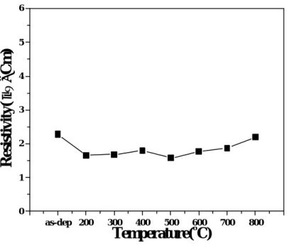
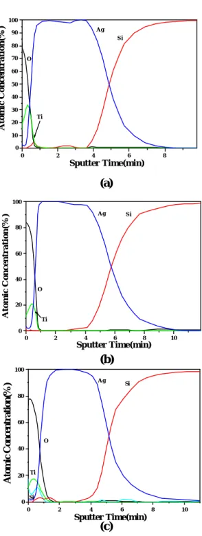
Fig .2 shows the resistivity of Ti/Ag/Si during vacuum annealing. It was deposited Ag on Si substrate and then deposited thin Ti subsequently. In 200℃ annealing, rapid drop of Ag is observed, however, after that, the resistivity remains constant up to 700℃annealing. From this resistivity result we can guess that Ag and Si has no reaction occurs. Ag was deposited on Si and the Ti is deposited subsequently on Ag. And then AES analysis were carried out. Fig. 3 were consisted with the Auger Electron Spectroscopy depth of Ti(700Å)/Ag(2000Å) /Si with as-deposited , 500℃
annealing and 700℃ annealing. From as-dep of AES in
Ti(700Å)/Ag(2000Å)/Si is shown the Ag peak and Si peak make a sharp line in the boundary and the sharp line of Ag and Si wouldn’t show any change until 700℃annealing. From this results, we can guess no reaction is occurred between Ag and Si layers. It causes no diffusion barrier is needed in Ag metallization process.Fig. 4 shows the resistivity variation of 2000Å-thick Ag(Mg) alloy film
Fig. 2. Resistivity variation of Ti(70Å)/Ag/Si with annealing temperature in vacuum.
as-dep 200 300 400 500 600 700 800 0
1 2 3 4 5 6
Resistivity(µΩ−Cm)
Temperature(oC)
Fig. 3. AES depth profiles of Ti(70Å)/Ag(2000Å)/Si annealed at various temp (a)as-dep, (b)500℃, and (c)700℃.
(a)
(b)
(c)
0 2 4 6 8
0 10 20 30 40 50 60 70 80 90 100
Ti O
S i A g
Atomic Concentration(%)
Sputter Time(min)
0 2 4 6 8 10
0 20 40 60 80 100
Ti O
A g S i
Atomic Concentration(%)
Sputter Time(min)
0 2 4 6 8 10
0 20 40 60 80 100
Si Ti
O
A g Si
Atomic Concentration(%)
Sputter Time(min)
on SiO2 coated wafer as functions of annealing temperature and Mg content.
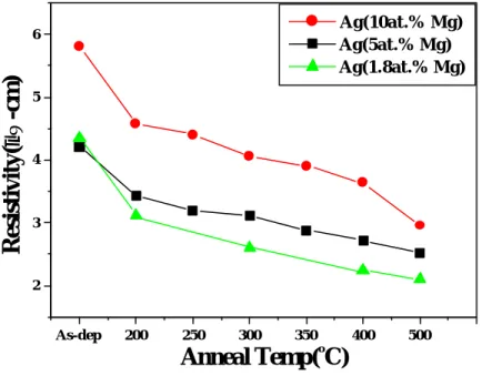
As the temperature increases from room temperature to 400℃, the resistivity decreases from 5.8 to 3.6μΩ-cm in Ag(10at.% Mg). Lowering Mg concentration reduces the resistivity further: Ag(5at.% Mg) and Ag(1.8at.% Mg) show the resistivities of 2.7, 2.2 μΩ-cm after annealing at 400℃. In addition, raising the temperature of Ag(10 at.% Mg) and Ag(5 at.% Mg) alloy films to 500℃ lowers the resistivity to 2.9, 2.5 μΩ-cm, respectively. Plan-view TEM of Ag(10at.% Mg) films revealed that the grain size of as-deposited Ag(Mg) film was 130Å. Increasing the temperature from 200℃ to 400℃ increased the grain size from 200Å to 420Å. Further increase of the temperature to 500℃ caused the rapid grain growth, achieving the average grain size of about 860Å. This grain growth is responsible for the rapid drop in resistivity. From these facts, it can be concluded that the decreased resistivity of Ag(Mg) alloy film with increasing the annealing temperature is mainly attributed to Ag grain growth and the residual Mg content in the film, and the grain growth can be
Fig. 4. Resistivity variation of Ag(Mg) alloy with annealing temperature and Mg concentration.
As-dep 200 250 300 350 400 500
2 3 4 5
6 Ag(10at.% Mg)
Ag(5at.% Mg) Ag(1.8at.% Mg)
Resistivity(µΩ-cm)
Anneal Temp(oC)
affected by the presence of Mg in Ag(Mg) film. AES analyses have been carried out to investigate Mg behavior in the Ag alloy films after annealing at high temperature. Fig. 5 shows AES depth profiles of Ag(10at.% Mg) alloy films/SiO2/Si after annealing in a vacuum at the temperature of 300 to 500℃. It can be seen the surface and interfacial Mg segregation. Heating the sample at 300℃ increases surface Mg content to about 42at.% from 18at.%, however, decreases interfacial Mg content. Raising the temperature to 400℃ causes a slight increase of surface Mg content and additional decrease of interfacial Mg content. However, increasing the annealing temperature to 500℃ allows the depletion of Ag from the free surface and additional increase of Mg near the surface, thus resulting in the formation of uniform MgO layer free of Ag. Ag-free MgO layer near the surface can be measured about 200Å and seems to be self-growth limited in Ag(Mg) alloy film.
In a vacuum of 10-5 Torr range, heating Ag(Mg) films, selective oxidation of Mg over Ag depends on the surface concentration of Mg and the reactivity of each element with oxygen. Oxygen is readily adsorbed on
Fig.5. Auger Depth profiles of Ag(10at.%Mg) films/SiO2 annealed in vacuum for 30min (a) as-dep, (b) 300℃, (c) 400℃, and (d) 500℃.
(c) (d)
(b) (a)
0 3 6 9
0 20 40 60 80 100
M g M g
S i
O
O A g
Atomic Concentration(%)
Sputter Time(min)
0 3 6 9
0 20 40 60 80 100
A g
O
O
S i
M g M g
Atomic Concentration(%)
Sputter Time(min)
0 2 4 6 8
0 20 40 60 80 100
O
S i
M g O
A g
Atomic Concentration(%)
S p u t t e r T i m e ( m i n )
0 5 10 15
0 20 40 60 80 100
M g
S i O A g
Atomic Concentration(%)
S p u t t e r T i m e ( m i n )
the surface of Ag, according to the reaction represented as
O2 + 2 Ag = 2 ( Ag-O) ---(1)
,where (Ag-O) represents an oxygen atom adsorbed on a surface site. This reaction probably competitively occurs on the surface with the reaction of oxygen with Mg. Considering the thermodynamic driving force, enthalpy and entropy of oxygen adsorption on silver are –108 Kcal/mol of oxygen, - 66 cal/mol/degree, respectively while enthalpy and entropy of MgO formation are –601.6 Kjoule/mol of oxygen, 143 joule/mol/degree, respectively. Therefore, it can be expected that as the temperature increases, the free energy of adsorption decreases more rapidly, thus less oxygen adsorption takes place on the silver site. In addition, higher temperature favors the more content of Mg near the surface due to the higher driving force for the segregation reaction and partly due to the enhanced mobility of Mg. This increased content of Mg allows selective oxidation of Mg over Ag.
In order to investigate the effects of annealing time on the resistivity of Ag(10at.% Mg) alloy film, vacuum annealing has been conducted as a function of time at the temperature of 400 and 500℃ as shown in Fig.6.
Fig. 6 Resistivity variation of Ag(10at.%Mg)alloy films annealed for 1.0 to 60min at 400℃ and 500℃, respectively.
0 10 20 30 40 50 60
2.4 2.8 3.2 3.6 4.0 4.4
500oC 400oC
1min3min as-dep
Resistivity(µΩ-cm)
Anneal Time(min)
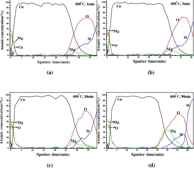
The resistivity decreases abruptly to 3.0 μΩ-cm, 2.7 μΩ-cm after 1 min of annealing at 400℃, 500℃, respectively and then slowly decreases for 10 min and finally remains constant until 60 min of annealing. This result can be compared with the dependence of Cu(Mg) alloy resistivity on annealing time in Cu(Mg)/SiO2/Si during annealing at the constant temperature of 400℃. Cu(Mg)/SiO2/Si shows a gradual increase in resistivity with time was observed at times longer than 20 minutes. AES depth profiles at several annealing times are shown in Fig. 7. It can be clearly seen that segregation of Mg occurred both at the free surface and at the SiO2 interface. As the annealing proceeds, Mg segregates preferentially near the Cu surface and the surface layer becomes progressively denser. However, after a dense MgO layer forms, substantial Mg segregation to the SiO2 interface takes place after, for example, 90 minutes of annealing, as seen in Fig. 7(d). Here, depletion of Si in the SiO2 near the interface proceeds, as indicated by a 100 Å gap between the onsets of silicon and oxygen at the interface. This can be attributed to some of the free Si generated from the reaction between Mg
and SiO2 dissolving in Cu and the
Fig. 7. AES depth profiles of Cu(4.5 at.% Mg)/SiO2/Si multilayers annealed in 10 mTorr of O for various annealing times; (a) 1 min, (b) 3 min, (c) 10
0 5 10 15 20 25 30 35
0 10 20 30 40 50 60 70 80 90
100 400oC, 1min
O
Si
Mg Mg
Cu C
Cu
Atomic concentration(%)
Sputter time(min)
0 5 10 15 20 25 30 35 40
0 10 20 30 40 50 60 70 80 90
100 400oC, 3min
C
O
Si
Mg O
Mg Cu
Atomic concentration(%)
Sputter time(min)
0 5 10 15 20 25 30 35
0 10 20 30 40 50 60 70 80 90
100 400oC, 10min
C
O
Si
Mg Mg
O Cu
Atomic concentration(%)
Sputter time(min)
0 5 10 15 20 25 30 35 40
0 10 20 30 40 50 60 70 80 90
100 400oC, 90min
Si O
Si
Mg Mg
O
C Cu
Atomic concentration(%)
Sputter time(min)
(a)
(c) (d)
(b)
min, and (d) 90 min.
other elements accumulating at the moving SiO2 interface.[25]
In contrast, Ag has negligible solubility of silicon, which limits Mg reaction with SiO2 and thus resulting in thinner MgO layer. AES depth profiles of the samples annealed at 400℃ for various annealing times are shown in Fig. 8. As the annealing of the sample proceeds, Mg moves near the surface and preferentially forms the surface MgO layer. Surface Mg concentration increases to about 42 at.% after 3 min of annealing and then slightly increases to 45 at.% after annealing for 60 min. In contrast, interfacial Mg content is not likely to increase with increasing annealing time, showing that limited interfacial reaction between Mg and SiO2 occurs, probably due to the negligible solubility of free silicon in Ag.
4. 2. Thermal Stress
Fig. 9 shows the stress variation of pure Ag and Ag(10at.%Mg) films of 1 ㎛ thickness, respectively, with temperature. During the first heating of Ag(10at.%Mg) alloy on Si, compressive stress resulting from differential
thermal expansion increases elastically until the stress relaxation starts in
Fig. 8. AES depth profile of Ag(10at.%Mg)/SiO2/Si (a)as-deposited and (a)
(b)
(c)
0 2 4 6 8 10 12 14 16
0 20 40 60 80 100
S i O
O M g
A g
Atomic Concentration(%)
S p u t t e r T i m e ( m i n )
0 2 4 6 8 10 12 14 16
0 20 40 60 80 100
S i O
O M g A g
Atomic Concentration(%)
S p u t t e r T i m e ( m i n )
0 2 4 6 8 10 12 14 16
0 20 40 60 80 100
S i O
OM g A g
Atomic Concentration(%)
S p u t t e r T i m e ( m i n )
then annealed at 400℃ for (b)3min and (c)60min, respectively.
Fig. 9. Stress variation of (a)pure Ag, (b)Ag(10at.%Mg) with annealing temperature.
Temp(oC)
0 100 200 300 400 500
Stress(MPa)
-200 -100 0 100 200 300 400
Temp(oC )
0 100 200 300 400 500
Stress(MPa)
-200 -100 0 100 200 300 400
(a)
(b)
the film around 120℃. This abrupt stress relaxation can be due to rapid grain growth in the film and predicted by Chaudhari’s equation below.
ó = áaE(1/Gi-1/Gf)/2(1-õ) --- (2)
where E is young’s modulus of the film and õ is Poisson’s ratio (0.33) of the film, Gi is initial grain size
TEM shows the first heating of Ag(10at.%Mg) film from 100℃ to 150℃ increases the average grain size from 47 nm to 59 nm in Fig. 10.
Substituting these values into equation (2) gives the stress change, which is comparable to the stress drop between 100℃ and 200℃, indicating that grain growth is responsible for the stress relaxation
Upon cooling from 420C, the stress increases elastically to about 220 MPa after a short range of rapid increase of stress. Second heating of the sample reduces the elastic tensile stress until about 150℃ and then causes a slight deviation from the thermoelastic line. Diffusional flow can be a dominant mechanism accounting for this plastic deformation occurring at this low stress range. Compared with in pure Ag, the increased diffusion flow
23
temperature is in part due to the solid solution effects on diffusion and
Fig. 10. Plan-view TEM of Ag(10at.%Mg)/TiN/Si annealed in vacuum.
As-dep (450Å ) 100℃ (510Å ) 150℃ (510Å )
200℃ (500Å ) 300℃ (1000Å ) 500℃ (1300Å )
50nm 50nm
50nm 50nm
50nm 50nm 100nm
in part due to MgO passivation limiting boundary dislocation’s mobility.
Similar results for passivated Cu film have been reported elsewhere by other groups, indicating that the presence of MgO on the surface acts as a passivation layer for Ag(Mg) films to limit the diffusional flow during a heating cycle. Upon second cooling from 420℃, the tensile stress elastically increases, similar to that from the first cooling cycle.
Comparing the stress-temperature curves of between pure Ag and Ag films shows that Ag film shows lower relaxation temperature on the first cycle. The relaxation of compressive stress is accompanied by grain growth, whose dominant mechanism in this temperature range is the coalescence of small grains in the compress-stressed film. Therefore, Mg alloying reduces Ag diffusivity, thus leading to slower grain growth as well as coalescence.
In addition, pure Ag shows much lower tensile stress and diffusional temperature as well. As a result, heating Ag(10at.%Mg)/SiO2 above 300℃
produces Mg-rich MgO on the surface, which acts as a passivation layer in air and supports high stress at room temperature and suppresses the
25
diffusional flow until 150℃.
4. 3. Adhesion
It is well known that poor adhesion to a glass substrate is an obstacle to the employment of silver in advanced TFT-LCDs, especially for bottom- gate-staggered a-Si:H TFT-LCDs. Silver is thermodynamically stable with Si and SiO2. To exam the annealing temperature effects on the adhesive force between Ag(Mg) alloy films and SiO2, Ag(10 at.% Mg) alloy films were deposited on SiO2 coated wafers and then annealed at the temperature of 100 to 400℃ and scratch-tested using a diamond tip. In addition, pure Ag/SiO2/Si sample was prepared as a reference to Ag(10at.% Mg) alloy film. Fig. 11 shows the critical loads obtained from the pure Ag/SiO2/Si and the Ag(10 at.% Mg)/SiO2/Si samples. Pure Ag film fails at approximately 13 N and the as-deposited Ag(10at.% Mg) alloy film on SiO2 shows the failure load of 30 N. This enhanced adhesion obtained from Ag(10 at.% Mg)/ SiO2 is attributed to the formation of the interfacial MgO layer resulting from Mg reaction with SiO2 near the interface. It is also noted that annealing the Ag(10 at.% Mg)/SiO2/Si multilayer structure at
various temperatures seems not to improve the adhesion property of
Fig. 11 Scratch images of pure Ag, Ag(10at.%Mg)/SiO2 with annealing.
(a) as-dep of pure Ag, (b) pure Ag annealed at 300℃, (c) Ag(10at.%Mg), (d) Ag(10at.%Mg) annealed at 300℃.
(a)
(b)
40N 40N
0 5 10 15 20 25 30 35 40
0 4 8 12 16 20
Acoustic Emission(a.u.)
L o a d ( N )
as-dep 300oC
Pure Ag
0 5 10 15 20 25 30 35 40
0 4 8 12 16 20
Acoustic Emission(a.u.)
L o a d ( N )
as-dep 300oC
Ag(10at.%Mg) (c)
(d)
Ag(10at.% Mg) to SiO2. The limited interfacial reaction can be responsible for the dependence of adhesion properties of Ag(10at.%
Mg)/SiO2/Si on annealing temperature.
As for Si substrate, there is not much difference in adhesion of between Ag and Ag(Mg), confirming that the reaction of Mg with SiO2 is a main contributor to the enhanced adhesion. It is also noted that Ag shows the better adhesion properties on SiO2 than on Si. It is because that Ag does not react with silicon to produce Ag silicide, but tends to react with oxygen to become Ag2O less than 100℃.
4. 4. O2 plasma treatment
To improve the adhesion strength, we treated the Si substrate with an O2 plasma at 130 mTorr for 5 min. The O2 plasma was created with O2/Ar flow ratio 25:0, 20:5, 15:10, and 0:25, RF powers of 150 W, at a fixed bias power of 30 W. For the scratch test, the Ag, and Ag(Mg) films deposited on the O2-plasma-treated Si were then annealed in a vacuum at 300℃ Fig.
28
12 show the resulting acoustic emission of annealed Ag, and Ag(Mg)
Fig. 12. Acoustic emission of (a) pure Ag, (b) Ag(10at.%Mg) on O2 plasma
0 5 10 15 20 25 30 35 40
0 10 20 30 40 50 60
Ar:O
2= 2 0 : 5 Ar:O
2=15:10 Ar:O2=0:25
Acoustic Emission
Load(N)
0 5 10 15 20 25 30 35 40
0 10 20 30 40 50 60
n o p l a s m a Ar:O2= 2 5 : 0 Ar:O
2= 2 0 : 5 Ar:O
2=15:10 Ar:O
2=0:25
Acoustic Emission
Load(N)
(a)
(b)
treated Si.
on the O2-plasma-treated Si, respectively. It can be clearly seen that significantly improved adhesion strength when Ar/O2 flow ratio 15:10. It was found that the adhesion strength of Ag-alloy films was generally improved at certain gas flow ratio. O2 plasma treatment, thus, produces excellent adhesion strength of Ag-alloy films to Si substrates. It is believed that the increased amount of oxygen at the interface between the film and the Si caused from O2 plasma treatment produces a strong reaction with the alloying element in the Ag-alloy film upon annealing, which leads to excellent film adhesion to the glass. From these results, it was concluded that O2 plasma treatment of the Si substrate followed by an annealing process provides significant improvements in adhesion strength.
Fig. 13 shows Cross-sectional TEM of Ag(Mg)/Si, revealing there is continuous oxide layer formed near the interface of between Ag(Mg) and Si.
The fact that ohmic contact is obtained with this structure indicates the oxide layer formed using O2 plasma act as an buffer layer to enhance the adhesion properties without sacrificing the contact resistance. The reaction
of Mg with thin oxide layer
Fig. 13. Cross-sectional TEM images of Ag(10at.%Mg) on O2 plasma Ag(Mg)
Ag(Mg)
Ag(Mg)
MgO(100Å )
100 Å 100Å
4. 5. Agglomeration
The films investigated were pure Ag, Ag(Mg). As-deposited films with thicknesses ranging from 500 to 2000Å were annealed in air at various temperatures from 200 to 400℃ for 10 min to investigate hillock growth and agglomeration of pure Ag films. (Fig. 14). After annealing, the films were examined by SEM. It was observed that annealing of the films caused hillock formation, hole growth, and agglomeration. The phenomenon of hillock formation appears to be caused by the relaxation of thermal stresses generated when the films are heated. Upon annealing, hillock formation appeared at lower temperatures and hole formation and agglomeration were observed at higher temperatures. As the pure Ag film thickness increased, complete agglomeration was observed at higher temperatures. The percentage of the resulting hole area on the surface of pure films in the 500 to 2000 Å thickness range on SiO2 at 300℃ was calculated and is plotted in Fig s. 15. In the case of the 500 Å Ag film, agglomeration occurred initially in the annealing process, and the extent of agglomeration remained
32
constant as the annealing process proceeded further.
Fig. 14. SEM micrograph of pure Ag on SiO2 annealed in air.
Ag 500Å Ag 1000Å Ag 2000Å
As-dep
200℃
300℃
400℃
1000 Å
2000 Å 500 Å
0 10 20 30 40 50 60
0 20 40 60 80 100
Hole Area(%)
Anneal Time(min)
Fig. 15. Variation of hole area formed on Ag films deposited on SiO2 upon annealing at 300℃ for various times.
34
In the case of the 1000Å Ag film, a period of hole growth appeared up to 3 minutes after annealing, and the Ag film agglomerated abruptly upon further annealing. No agglomeration was observed at the beginning of the annealing process in the 2000- Å Ag film. After 20 min, the holes continued to grow and join together, leading to the formation of separate islands and severe agglomeration.
To investigate the effects of self-aligned MgO obtained from Ag (Mg) alloys, we annealed as-deposited Ag(Mg) and MgO/Ag(Mg) films in air at
various temperatures from 200 to 500℃. As the as-deposited Ag(Mg) were annealed with temperatures up to 300 °C, the amount of Mg moving
to the Ag surface increased, resulting in an incremental increase of the MgO layer thickness. The surface segregation of Mg is probably due to the lower surface energy of Mg and its high reactivity with oxygen, which favors a preferential oxidation of Mg to form MgO. A self-aligned MgO layer was formed by annealing in vacuum at 300℃ for 30 min. Fig. 16 shows the sheet resistance variation of as-deposited pure Ag/SiO2 and
35
preannealed Ag(10at.% Mg) / SiO2 after annealing in air at 200 to 500℃.
Ag(Mg) alloy films/SiO2 was pre-annealed in vacuum at 300℃. In addition, the thickness of pure Ag and Ag(Mg) alloy films was 1000Å. It can be seen that the sheet resistance of pure Ag significantly increases after annealing at 300℃. On the contrary, the pre-annealed Ag(Mg)/SiO2 shows a constant resistance until 500℃, implying that the surface MgO layer formed on the Ag surface after annealing at 300℃ enables sufficient resistance to agglomeration.
Thus, the self-aligned MgO layer obtained from Ag (Mg) alloy film can enhance the resistance to agglomeration.
Fig. 16. Sheet resistance variation of a 1000Å-thick and Ag(Mg)/SiO2
annealed in vacuum at 300℃ as a function of annealing temp.
As-dep 200 300 400 500
0.0 0.5 1.0 1.5 2.0 2.5
Pure Ag
Ag(Mg) annealed at 300oC
Sheet Resistance( Ω /sq)
Temperature(
oC)
37
5. Conclusion
Ag(Mg) alloy films have been sputter-deposited on SiO2 coated wafers and characterized. Annealing Ag(10at.% Mg)/SiO2/Si at 300℃ or higher allowed the preferential segregation of Mg to the surface and the depletion of Ag from the free surface, leading to the formation of (Mg, Ag)O layer near the surface and providing the agglomeration resistance in air. A dense MgO layer (approximately 150-200Å) free of Ag was produced after annealing at 500℃. In addition, adhesion of Ag(Mg) to SiO2 was significantly improved and not affected by annealing temperature. This can be explained by the formation of the limited-thickness interfacial MgO layer, independent of annealing temperature. The resistivity of Ag(Mg) alloy film depends on Mg content and annealing temperature; the resistivity of Ag(10at.Mg) alloy film was decreased to 2.9 μΩ-cm after annealing at 500℃ and lowering Mg content to 1.8 at.% reduced the resistivity to 2.1μ Ω-cm.
38
6. Reference
[1] N. Ibaraki, Materials Chemistry and Physics 43 220 (1996).
[2] W. E. Howard, J. Soc. Inform. Display 3 127 (1995).
[3] H. Sirringhaus, S. D. Theiss, A. Kahn, and S. Wagner, IEEE Electorn Device Lett. 18 August (1997).
[4] N. Hirano, N. Ikeda, H. Yamafuchi, S. Nishida, Y. Hirai and S. Kaneko, Conf. Record 1994 IDRC 369 (1994).
[5] H. Morimoto, Proc. 12th IDRC 337 (1992).
[6] I.J. Chung, IDMC 2000, 155 (2000).
[7] Y. Wang and T. L. Alford, Appl. Phys. Lett. 74, 52 (1999).
[8] Phucanh Nguyen, Yuxiao Zeng, and T.L. Alford, J.Vac.Sci.Technol.B 19(1), 158 (2001).
[9] C.O. Jeong, N.S. Roh, S.G. Kim, H.S. Park, C.W. Kim, D.S. Sakong, J.H. Seok, K.H. Chung, W.H. Lee, Dongwen Gan, Paul S. ho, B.S. Cho, B.J. Kang, H.J. Yang, Y.K. Ko, and J.G. Lee, “Feasibility of an Ag- alloy Film as a Thin Film Transistor Liquid Crystal display”, submitted.
39
[10] M. Hauder, J. Gstottner, W. Hansch, and D. Schmitt-Landsiedel, Appl.
Phys. Lett. 78, 838 (2001).
[11] E. Kondoh and T. Asano, “Material issues in silver metallization”, Conference Proceedings ULSI XV, Materials Research society, 219 (2000).
[12] T. Laursen, Daniel Adams, T. L. Alford, K-N. Tu, F. Deng, R. Morton, and S. S. Lau, Thin Solid Films 290-291, 411 (1996).
[13] Y. Wang and T. L. Alford, Appl. Phys. Lett. 74, 52 (1999).
[14] T. L. Alford, J. Le, J. W. Mayer, and S. Q. Wang, Thin Solid Films, 262 (1995).
[15] T. L. Alford, D. Adams, T. Laursen, and B. M. Ullrich, Appl. Phys.
Lett. 68, 23 (1996).
[16] W. H. Lee, H. L. Cho, B. S. Cho, J. Y. Kim, Y-S. Kim, W-G. Jung, H.
Kwon, J. H. Lee, C. M. Lee, P. J. Reucroft, and J. G. Lee, J.
Electrochem. Soc. 147(8), 3066 (2000).
[17] W. H. Lee, H. L. Cho, B. S. Cho, J. Y. Kim, Y-S. Kim, W-G. Jung, H.
Kwon, J. H. Lee, C. M. Lee, P. J. Reucroft, and J. G. Lee, J. Vac. Sci.
Technol. A 18(6), 2972 (2000).
[18] W. H. Lee, H. L. Cho, B. S. Cho, J. Y. Kim, Y-S. Kim, W-G. Jung, H.
Kwon, J. H. Lee, C. M. Lee, P. J. Reucroft, E. G. Lee, and J. G. Lee, Appl. Phys. Lett. 77(14), 2192 (2000).
[19] J.G. Lee, H.G. Cho, E. G. Lee, J. G. Lee, K. B. Kim, and J. M. Lee, Journal of the Korean Physical Society, 35, p.s65 – s70 (1999).
[20] P. S. Shin, T. C. Chang, S. M. Chen, M. S. Feng, D. Z. Peng, and C. Y.
Chang, Surf. and Coating Technol. 108, 588 (1998).
[21] P.J. Ding, W.A. Lanford, S. Hymes, and S.P. Murarka, J. Appl. Phys., 75, 3627 (1994).
[22] P.J. Ding, W.A. Lanford, S. Hymes, and S.P. Murarka, Appl. Phys. Lett., 64(21), 2897 (1994).
[23] W. Wang, P.J. ding, s.Hymes, S.P. Murarka and W.A. Lanford, private communication, (1994).
[24] W.A. Lanford, P.J. Ding, W. Wang, S. Hymes, and S.P. Murarka, Thin Solid Films, 262, 234 (1995).
[25] H.L. Cho and J.G. Lee, MRS Proceedings, spring, 7 (1999).