• 검색 결과가 없습니다.

Novel Low-Volume Solder-on-Pad Process for Fine Pitch Cu Pillar Bump Interconnection

N/A
N/A
Protected

Academic year: 2021

Share "Novel Low-Volume Solder-on-Pad Process for Fine Pitch Cu Pillar Bump Interconnection"

Copied!
5
0
0

로드 중.... (전체 텍스트 보기)

전체 글

(1)

Novel Low-Volume Solder-on-Pad Process for Fine Pitch Cu Pillar Bump Interconnection

Hyun-Cheol Bae

, Haksun Lee, Yong-Sung Eom and Kwang-Seong Choi

Energy Harvesting Devices Research Section, Information & Communications Core Technology Research Laboratory 218, Gajeong-ro, Yuseong-gu, Daejeon 305-700, Korea

(Received June 10, 2015: Corrected June 17, 2015: Accepted June 19, 2015)

Abstract: Novel low-volume solder-on-pad (SoP) process is proposed for a fine pitch Cu pillar bump interconnection.

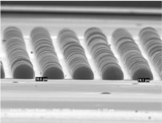
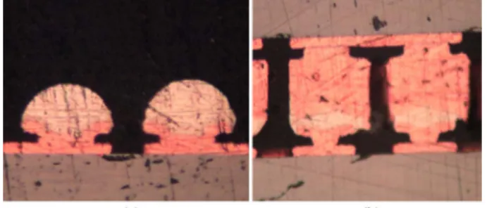
A novel solder bumping material (SBM) has been developed for the 60 µm pitch SoP using screen printing process. SBM, which is composed of ternary Sn-3.0Ag-0.5Cu (SAC305) solder powder and a polymer resin, is a paste material to perform a fine-pitch SoP in place of the electroplating process. By optimizing the volumetric ratio of the resin, deoxidizing agent, and SAC305 solder powder; the oxide layers on the solder powder and Cu pads are successfully removed during the bumping process without additional treatment or equipment. The Si chip and substrate with daisy-chain pattern are fab- ricated to develop the fine pitch SoP process and evaluate the fine-pitch interconnection. The fabricated Si substrate has 6724 under bump metallization (UBM) with a 45 µm diameter and 60 µm pitch. The Si chip with Cu pillar bump is flip chip bonded with the SoP formed substrate using an underfill material with fluxing features. Using the fluxing underfill material is advantageous since it eliminates the flux cleaning process and capillary flow process of underfill. The optimized interconnection process has been validated by the electrical characterization of the daisy-chain pattern. This work is the first report on a successful operation of a fine-pitch SoP and micro bump interconnection using a screen printing process.

Keywords: solder-on-pad, fine pitch bumping, micro bump interconnection

1. Introduction

For high performance electronic products, more dense integration and short interconnection is required. To obtain the high-density I/Os and low signal loss, 3D die intercon- nection is a key technology. More dense integration and increasing number of IOs implies scaling down the micro bump dimension and pitch. Tight control for the perform- ing process of micro bump and stacking accuracy are required. Several methods for interconnection micro bumps with a fine pitch have attempted, such as Cu(Ni)Sn Cu pil- lar with solder cap, Cu-Cu direct bonding and Transient liquid phase (TLP) CuSn bump.

1-6)

Direct Cu-Cu bonding is needed relatively high bonding temperature and pressure in spite of high throughput.

3)

Transient liquid phase (TLP) CuSn bonding is a promising process for low temperature thermo-compression bonding process that transforms sol- der into high melting point intermetallic (IMC) bonds.

4)

In view of obtaining high reliable micro bump, Cu pillar with solder cap using electro plating or electroless plating

method is commonly used. The electroplating process for micro bump, it is very hard to obtain SAC305 solder cap.

Therefore, cost-effective SAC305 SoP process using the screen printing is very attractive. Solder cap process is per- formed on the Cu pillar bump. The presented SoP is formed on the under bump metallization (UBM) layer in substrate.

Also, flux and underfill materials are the most critical components for a reliable flip-chip bonding process using micro bumps. For flux-applying process, however, clean- ing of flux residue is another issue after flip-chip bonding process. The flux residue is unfavorable for following underfill dispensing process, and can further make a long- term reliability issue. Therefore, the development of flip- chip bonding process without the usage of flux for the join- ing of micro bumps is required.

In this paper, the developed fine pitch SoP process and interconnection process for fine pitch micro bump is newly presented. This fine pitch SAC305 SoP process is devel- oped using a maskless screen printing.

Corresponding author E-mail: [email protected]

© 2015, The Korean Microelectronics and Packaging Society

This is an Open-Access article distributed under the terms of the Creative Commons Attribution Non-Commercial License(http://creativecommons.org/

licenses/by-nc/3.0) which permits unrestricted non-commercial use, distribution, and reproduction in any medium, provided the original work is

properly cited.

(2)

Since the micro bump interconnection needs fine pitch and low-volume solder bump, a novel maskless solder bump maker (SBM) is developed.

7-13)

The SBM, which is composed of solder powder and polymer resin, is the mate- rial that pastes or binds the solder bump on a given sub- strate. Particularly, the polymer resin for the SBM has the function of removing oxide layers existing on the surface of the solder powder and Cu pad during the bumping pro- cess. In this work, Sn-3.0Ag-0.5Cu (SAC305) powdered solder is blended with the resin. The specification of the distribution of the solder diameters for type 7 and type 8 are according to the standard:

14)

2 μm to 11 μm and 2 μm to 8 μm with weight percentages of 90% for type 7 and type 8, respectively.

The type 8 solder powder is newly adopted. From the previous results, the type 7 solder powder is usually used because the minimum bump pitch is over than 130 μm.

10-12)

Using numerical estimation, the number of solder particles placed on the Cu pad area is calculated. When type 7 sol- der powder is used, 48 solder particles can be placed on a Cu pad with diameter of 45 μm. Similarly, for type 8, 81 solder particles can be placed on the same pad area.

The volumetric mixing ratio between the polymer resin and the SAC305 solder powder is 86:14. The mixing ratio is analyzed to establish a proper interaction between the solder powder and the Cu pads, and optimized fully to fill the Cu pads. Figure 1 shows the whole bumping process for the fine pitch SoP process. SBM material is printed on the Si substrate, and printed area and thickness is con- trolled by a guide. This guide is not a patterned mask, as opposed to a photoresist mask or a metal mask which defines the open areas or separates the micro bumps. The reflow process is performed at 270

o

С for 40 sec. in an IR oven. After reflow process, the residue and solder particles are cleaned off in ultrasonic baths of MIF, acetone, and methanol for several minutes. While previous works required processes such as a second resin printing, clean- ing, and coining, this proposed SoP process does not require such processes.

10,11)

The test vehicles are fabricated to develop the fine pitch SoP process using SBM material and screen printing pro- cess. For its demonstration, Si chip and substrate are fabri- cated with a daisy-chain pattern. The 7 mm × 7 mm Si chip is fabricated with 6724 Cu pillars, which have a pitch of 60 μm. The used Cu pillars have the diameter of 45 μm and the height of 30 μm, as shown in Fig. 2(a). Moreover Si substrate having the same number of Cu pads is also fabri-

cated to form the 60 μm pitch SoP, as shown in Fig. 2(b).

The used Cu pads have a 5 μm TiW/Cu under bump met- Fig. 1. Process flow of fine pitch SoP using screen printing.

Fig. 2. Photograph and SEM images of daisy-chain test vehicle:

(a) fabricated Si chip with Cu pillars, and (b) fabricated Si

substrate with UBM.

(3)

allization (UBM) layer, which has a diameter of 45 μm.

The optical images of the fabricated Si substrate are shown in Fig. 3. The size of the used Si substrate is 15 mm

× 15 mm. The fabricated Si substrate after SoP process is covered with SAC305 solder bumps as shown in Fig. 3(b).

No solder bridges which are easily formed by maskless printing process are found in the Fig. 3(c). From the scan- ning electron microscope (SEM) image of the formed fine pitch SoP array, the 60 μm pitch SoPs are well formed on the UBM layers with uniform shapes. Also, all 6724 Cu pads are fully filled without any missing bumps, as shown in Fig. 4.

3. Fine Pitch Interconnection Process

The test vehicles are flip-chip bonded, and the bonding process flow is very simple. To begin with, a developed

fluxing underfill, which does not need a clean step, is applied to the Si substrate. The fluxing underfill material has the fluxing and the capillary underfill features.

15-17)

In this material, deoxidizing agents together with a hardener are added to the underfill to form an epoxy-based thermo- set. Then the Si chip with the Cu pillar bumps is aligned to the Si substrate with SoPs, and the solder joints are all formed simultaneously using the thermo-compressing bonding. During the flip chip bonding, additional flux cleaning and capillary action are not required. The opti- mized bumping and interconnection processes have been validated by an electrical characterization of the daisy- chain patterned test vehicles. Figure 5 shows the photo- graph of the flip-chip bonded test vehicle. Different bond- ing conditions (bonding temperature, time, and pressure) are examined to achieve the best joining result. The fabri- cated Si chip and substrate are well bonded with the devel- oped fluxing underfill material. First, fluxing underfill is dispensed onto the Si substrate and preheated at 120

o

С for 10 seconds. Next, the pressure of 200 gf is applied onto the joint while the temperature is set to 250

o

С for 20 seconds.

The fine pitch interconnection between Cu pillars and SoP is checked using two quick analysis methods. One is the cross-section inspection of the bonded chip and sub- strate, as shown in Figs. 6(a) and 6(b). Figures 6(a) and Fig. 3. Optical images of fabricated Si substrates: (a) before, (b)

after SoP forming process and (c) magnification of (b).

Fig. 4. SEM image of fully formed SAC SoPs on the 6724 Cu pads.

Fig. 5. Photograph of flip-chip bonded test vehicle.

(4)

6(b) show the cross-sectional views of the SoP and Cu pil- lar interconnections before and after the bonding process.

From the cross-section inspection, the bump shape and height information of SoP obtained through an SEM vir- tual inspection are verified. Cu pillars and SoP are properly interconnected without an alignment issue. Electrical defects commonly occur in fine pitch bonding when the adjacent bumps make an electrical short effect or when an insufficient volume of solder creates an electrical opening effect. However, no such electrical defects are found in these fine pitch Cu pillar bump interconnections. The other method used to check the fine pitch interconnection is to compare the calculated and measured resistance values of the test vehicles with the daisy chain patterns, as shown in Figs. The measured DC resistance values are compared with the calculated resistances of the test vehicles with the daisy-chain patterns, as shown in Fig. 5 and 7. The bonded test vehicles are designed to connect all of the bumps and have six DC probing pads. In detail, total 6724 bump inter- connection is checked by probing top pad and bottom pad, marked as number 1 and 6 respectively. The right and left pads are designed to inspect the internal bump open and short effects. If the test vehicles are well bonded, the DC resistance values will show an increasing tendency as the section goes from 1-2 to 1-6.

The simple DC resistance values can be calculated with Eq. (1)

(1)

Here R

TOTAL

is total sum of the resistance values, ρ is resistivity of metal and solder, L is length and A is cross- sectional area. The resistance values of redistribution layer (RDL) of Si chip, the interconnection bumps between the chip and substrate, and the RDL of Si substrate are included in R

TOTAL

. Values L and A respectively represent the length and area of all the interconnection paths. The calculated and measured DC resistances values of the test

vehicle, reflecting 6,724 bump interconnections, are sum- marized in Table 1. From the comparison results, it is obvi- ously proved that the interconnection of Cu pillars and SoPs is successful. This measured DC resistance values have some variations of contact resistance.

4. Conclusion

A fine pitch solder-on-pad process using a screen print- ing process was newly presented and successfully devel- oped by optimizing the volumetric mixing ratio between resin and Sn-3.0Ag-0.5Cu solder powder. The test vehicles with daisy-chain pattern were fabricated to evaluate the presented SoP technology and the simple interconnection process using a fluxing underfill material. From SEM images and the DC resistance measurement data, presented bumping technology and fine pitch micro bump intercon- nection were verified. Therefore, because of the simplicity and cost-effectiveness of the process, the developed SoP technology can be used instead of solder cap process with electroplating.

Acknowledgements

This work was supported by R&D program Electronics and Telecommunications Research Institute (ETRI) [ESSOP:

Extremely Small System-on-Packaging] and by R&D pro- gram of ISTK [Development of an image-based, real-time inspection and isolation system for hyperfine faults].

R

TOTAL

= ρ L A ---

×

Fig. 6. Cross-sectional images of the Si substrate: (a) before and (b) after flip chip bonding process.

Fig. 7. Schematic of DC resistance calculation of daisy-chain pat- terned test vehicles.

Table 1. Comparison of DC resistance values between calculated results and measured data

Section Measured Resistance ( Ω)

Total measured resistance ( Ω)

Total calculated resistance ( Ω)

1-2 6

36.8 32.3

1-3 17.3

1-4 24.6

1-5 31.1

1-6 36.8

(5)

References

1. A. Yu, J. H. Lau, S. W. Ho, A. Kumar, W. Y. Hnin, W. S.

Lee, M. C. Jong, V. N. Sekhar, V. Kripesh, D. Pinjala, S.

Chen, C.-F. Chan, C.-C. Chao, C.-H. Chiu, C.-M. Huang and C. Chen, “Fabrication of High Aspect Ratio TSV and Assem- bly with Fine-Pitch Low-Cost Solder Microbump for Si Inter- poser Technology with High-Density Interconnects”, IEEE Transactions on Components, Packaging, Manufacturing Technologies (CPMT), 1(9), 1336 (2011).

2. Y. Orii, K. Toriyama, H. Noma, Y. Oyama, H. Nishiwaki, M.

Ishida, T. Nishio, N. C. Labianca and C. Feger, “Ultrafine- pitch C2 Flip Chip Interconnections with Solder-Capped Cu Pillar Bumps”, Proc. of the 59

th

Electronic Components and Technology Conference (ECTC), 948 (2009).

3. Y. H. Hu, C. S. Liu, M. J. Lii, A. L. Manna, K. J. Rebibis and M. Zhao, “3D Stacking Using Cu-Cu Direct Bonding for 40 µm Pitch and Beyond”, Proc. of the 4

th

European System Integration Technology Conference (ESTC), (2012).

4. R. Agarwal, W. Zhang, P. Limaye and W. Ruythooren, “High Density Cu-Sn TLP Bonding for 3D Integration”, Proc. of the 59

th

Electronic Components and Technology Conference (ECTC), 345, (2009).

5. M. S. Kim, Y. H. Ko, J. H. Bang and C. W. Lee, “The Chip Bonding Technology on Flexible Substrate by Using Micro Lead-free Solder Bump”, J. Microelectron. Packag. Soc., 19(3), 15 (2012).

6. J. B. Kim, S. H. Kim and Y. B. Park, “Intermetallic Com- pound Growth Characteristics of Cu/Ni/Au/Sn-Ag/Cu Micro- bump for 3-D IC Packages”, J. Microelectron. Packag. Soc., 20(2), 59 (2013).

7. K.-S. Choi, K. J. Sung, B. O. Lim, H. C. Bae, S. Jung, J. T.

Moon and Y. S. Eom, “Novel Maskless Bumping Material for 3D Integration”, ETRI J., 32(2), 342 (2010).

8. K.-S. Choi, S. W. Chu, J. J. Lee, K. J. Sung, H. C. Bae, B.

O. Lim, J. T. Moon and Y. S. Eom, “Novel Bumping Material for Solder-on-Pad Technology”, ETRI J., 33(4), 637 (2011).

9. Y.-S. Eom, K. S. Choi, S.-H. Moon, J. H. Park, J. H. Lee and J. T. Moon, “Characterization of a Hybrid Cu Paste as an Iso- tropic Conductive Adhesive”, ETRI J., 33(6), 864 (2011).

10. K.-J. Sung, K. S. Choi, H. C. Bae, Y. H. Kwon and Y. S. Eom,

“Novel Bumping and Underfill Technologies for 3D IC Inte- gration”, ETRI J., 34(5), 706 (2012).

11. K.-S. Choi, H. E. Bae, H. C. Bae and Y. S. Eom, “Novel Bumping Process for Solder on Pad Technology”, ETRI J., 35(2), 340 (2013).

12. Y.-S. Eom, J. H. Son, H. C. Bae, K. S. Choi and H. S. Choi,

“Optimization of material and process for fine pitch LVSoP technology”, ETRI J., 35(4), 625 (2013).

13. J.-H. Son, Y.-S. Eom, K.-S. Choi, H. S. Lee, H. C. Bae and J. H. Lee, “HV-SoP Technology for Maskless Fine Pitch Bumping Process”, ETRI J., 37(3), 523 (2015).

14. IPC Std. J-STD-005, “Requirements for Soldering Pastes”.

15. Y.-S. Eom, J. W. Back, J. T. Moon, J. D. Nam and J. M. Kim

“Characterization of Polymer Matrix and Low Melting Point Solder for Anisotropic Conductive Film”, Microelectron.

Eng., 85, 327 (2008).

16. Y.-S. Eom, K.-S. Jang, J.-T. Moon and J. D. Nam, “Electrical Interconnection with a Smart ACA Composed of Fluxing Polymer and Solder Powder”, ETRI J., 32(3), 414 (2010).

17. Y.-S. Eom, J.-H. Son, K.-S. Jang, H. S. Lee, H. C. Bae and

J. H. Lee, “Characterization of fluxing and hybrid underfills

with micro-encapsulated catalyst for long pot life”, ETRI J.,

36(3), 343 (2014).

수치

Fig. 2. Photograph and SEM images of daisy-chain test vehicle:
Fig. 4. SEM image of fully formed SAC SoPs on the 6724 Cu pads.
Fig. 7. Schematic of DC resistance calculation of daisy-chain pat- pat-terned test vehicles.

참조

관련 문서

So, we proposed a novel method for video event analysis and description on the fundamental of the Domain Knowledge object ontology, the MPEG-7 standard is extended

<Ohyouranjeon> was understood that it has the history of literature meaning of selling out novel on the transitional period of the old novel and

The study was made to reduce the weight of the body by using Friction Stir Welding (FSW), which is a solid joining process of low heat input type in order to solve

The purpose of this study is to fine out the reason of which non-regular workers have been increased since the crisis, to show some problems of their

In addition, this study confirmed the superiority of the thermomechanical reliability of drilled Cu pillar bump (DCPB) through a hysteresis loop, which showed the

(6) Choice of fine aggregate content (S/a, 잔골재율 ) with known volumes of coarse aggregate, water, cement and air & Unit water mass. (7) Estimation of unit volume of

~ a volume which is fixed in space and through whose boundary matter, mass, momentum, energy can flow. ~ The boundary of control volume is

The main feature of the formulation is the use of an integral approach for obtaining the velocity and pressure fields, in conjunction with a finite volume scheme and the