• 검색 결과가 없습니다.

Improvement in Thermomechanical Reliability of Power Conversion Modules Using SiC Power Semiconductors: A Comparison of SiC and Si via FEM Simulation

N/A
N/A
Protected

Academic year: 2021

Share "Improvement in Thermomechanical Reliability of Power Conversion Modules Using SiC Power Semiconductors: A Comparison of SiC and Si via FEM Simulation"

Copied!
10
0
0

로드 중.... (전체 텍스트 보기)

전체 글

(1)

Improvement in Thermomechanical Reliability of Power Conversion Modules Using SiC Power Semiconductors: A Comparison of SiC and Si via FEM Simulation

Cheolgyu Kim

1

, Chulmin Oh

2

, Yunhwa Choi

3

, Kyung-Oun Jang

4

, and Taek-Soo Kim

1,†

1

Department of Mechanical Engineering, Korea Advanced Institute of Science and Technology (KAIST), 291, Daehak-ro, Yuseong-gu, Daejeon 34141, Korea

2

Electronic Convergence Material & Device Research Center, Korea Electronic Technology Institute, Saenari-ro, Bundang-gu, Seongnam-si, Gyeonggi-do 13509, Korea

3

JMJ Korea Co., Ltd., 102, Gilju-ro 425beon-gil, Bucheon-si, Gyeonggi-do 14487, Korea

4

Power conversion, Fairchild Semiconductor Ltd., 55, Pyeongcheon-ro 850beon-gil, Bucheon-si, Gyeonggi-do 14487, Korea (Received July 24, 2018: Corrected September 17, 2018: Accepted September 20, 2018)

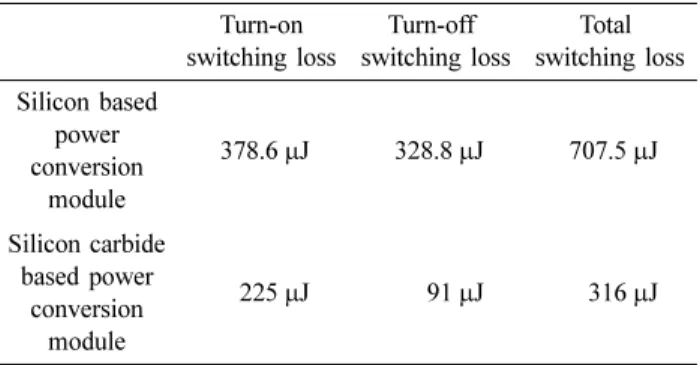
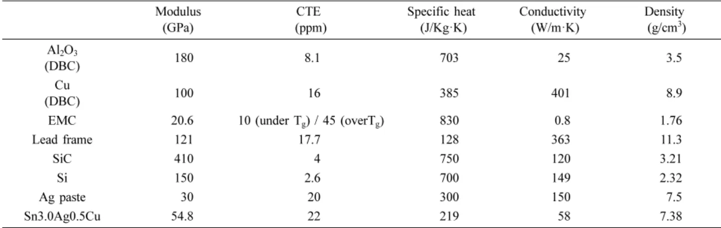
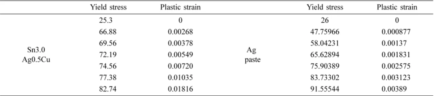
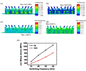
Abstract: Driven by the recent energy saving trend, conventional silicon based power conversion modules are being replaced by modules using silicon carbide. Previous papers have focused mainly on the electrical advantages of silicon carbide semiconductors that can be used to design switching devices with much lower losses than conventional silicon based devices. However, no systematic study of their thermomechanical reliability in power conversion modules using finite element method (FEM) simulation has been presented. In this paper, silicon and silicon carbide based power devices with three-phase switching were designed and compared from the viewpoint of thermomechanical reliability. The switching loss of power conversion module was measured by the switching loss evaluation system and measured switching loss data was used for the thermal FEM simulation. Temperature and stress/strain distributions were analyzed. Finally, a thermal fatigue simulation was conducted to analyze the creep phenomenon of the joining materials. It was shown that at the working frequency of 20 kHz, the maximum temperature and stress of the power conversion module with SiC chips were reduced by 56% and 47%, respectively, compared with Si chips. In addition, the creep equivalent strain of joining material in SiC chip was reduced by 53% after thermal cycle, compared with the joining material in Si chip.

Keywords: Power conversion module, silicon carbide (SiC), switching loss, thermal FEM simulation, thermomechanical reliability

1. Introduction

A power conversion module is a module in which two or more power devices and control ICs are packaged. Power devices are semiconductor devices used for power conver- sion and power control, and consist of diodes, power transis- tors, MOSFETs, IGBTs, and thyristors. They are typically classified as either switching elements, which are capable of on-off operation, or rectifiers, which provide rectification.

Power conversion modules are commonly used in air con- ditioners, refrigerators, washing machines and other energy consuming home appliances. Recent concerns for energy saving and conservation, CO

2

regulation, and protection of the environment have stimulated the development of higher efficiency and more environmentally friendly power semiconductor devices, and research is being actively car-

ried out in the field to improve performance. Among the types of energy losses that occur in power conversion devices, switching losses and conduction losses tend to be the largest.

1)

Switching losses occur when the device is transitioning from the blocking state to the conducting state and vice-versa. This interval is characterized by a signifi- cant voltage across the switch’s terminals and a significant current through it. To determine the switching losses of a device, the energy dissipated in each transition needs to be multiplied by the switching frequency. Conduction losses occur when the device is operating and current is flowing.

Those losses are in direct relation to the duty cycle.

The silicon-based power conversion module, which has been in operation for more than 40 years, has now reached its theoretical performance limit, and to improve power conversion efficiency, power conversion modules based on

Corresponding author E-mail: [email protected]

© 2018, The Korean Microelectronics and Packaging Society

This is an Open-Access article distributed under the terms of the Creative Commons Attribution Non-Commercial License(http://creativecommons.org/

licenses/by-nc/3.0) which permits unrestricted non-commercial use, distribution, and reproduction in any medium, provided the original work is

properly cited.

(2)

wide band gap materials such as silicon carbide (SiC) or gallium nitride (GaN) compound semiconductors are being developed.

2-4)

Silicon carbide based devices are expect to significantly reduce on-resistance compared to conven- tional silicon power semiconductors, and also reduce the size of inductors and capacitors, due to their high switching frequency characteristics compared with silicon.

5-7)

The sil- icon carbide based devices are capable of high temperature switching at high temperatures because of their high tem- perature stability, high bandgap, insulation resistance, and high breakdown field voltage, compared to existing silicon devices.

8-12)

It is expected that the resulting reduction in the size of the high-frequency filter and the number of compo- nents will make it possible to miniaturize the design of the power module system. The features of the cooling system for the power conversion module can also be greatly reduced due to the reduction in the volume of the module, and its high temperature operating characteristics. By vir- tue of its low resistance and high withstand voltage, high- frequency characteristics are also possible, superior to those of the MOSFETs and IGBTs in existing silicon based low-power power conversion modules. Accordingly, ther- momechanical reliability is important to ensure the system operates stably. In order to take advantage of the silicon carbide device characteristics, a high-density packaging, low thermal resistance and high temperature tolerant power module structure needs to be developed. Also, the thermo- mechanical reliability of the power module should remain high under high temperature operating conditions.

However, previous studies have mainly focused on inves- tigating electrical properties, and there are not many papers focusing on thermomechanical reliability.

13-15)

Among them, few papers have focused on finite element method (FEM) simulations which consider only the temperature distribu- tion of the power module.

16-18)

In this paper, we discuss the process of evaluating the thermomechanical reliability of two types of power conversion modules using thermal FEM simulations. Two main losses, the conduction loss and switching loss, should be considered in order to analy- sis thermomechanical characteristic induced by the power losses. However, in this paper, only switching loss is con- sidered due to the scope of research. The switching losses of silicon and silicon carbide based power conversion mod- ules were quantitatively measured using a switching loss evaluation system. Using the measured switching losses and the heat flux, the thermal loading conditions for the simulation were calculated for various working frequen- cies. A thermal transfer simulation was also conducted to evaluate the maximum operating temperature of the

devices and its location. The temperature distribution cal- culated using the thermal transfer simulation was then used as the thermal loading data for a thermal stress simulation.

Finally, a thermal simulation was performed to evaluate creep damage in the chip joining materials.

2. Experiments

Most household appliances have a three-phase switching device, and a total of six switching elements are mounted to control their three-phase motors.

19,20)

The low-power power conversion module, which consists of six switching elements and diodes, is mounted on a lead frame in the form of a bare chip with three control ICs. For this study, prototypes of silicon and silicon carbide based power con- version modules were designed. The switching devices and diodes used in the power conversion modules were bare chip type. The silicon based power conversion module uti- lized a Si IGBT (600-V, 30-A, Trinno, TGAN30N60FDR) and Si diode (600-V, 30-A, Trinno TD30B60WX). Six IGBTs and six diodes were placed on direct-bonded-copper (DBC). Each control IC was in charge of one-phase of switching. The control IC was a packaged product using a surface-mount technology structure and was mounted on a printed circuit board (PCB) substrate. Using the switching devices and rectifiers, the circuit design of the silicon based power conversion module was composed of 3 phases (U, V, W) as shown in Fig. 1(a). One control IC, with two IGBTs and two diodes, was designed to correspond to each phase. Based on the circuit design, a wire diagram for the wire connection and PCB wiring between each device was designed, and the size of the module and the size of each pin were determined. For the attachment process, commer- cial solder (Sn-3.0Ag-0.5Cu composition) was used. The DBC substrate was placed on the mounting guide, and then the solder was placed on the DBC substrate to bond the chips using a vacuum reflow process.

For the silicon carbide based power conversion module,

a SiC MOSFET (900-V, 36-A, Cree CPM3-0900-0065B)

and SiC diode (650-V, 30-A, Cree diode CPW5-0650-

Z030B) were used as shown in Fig. 1(b). For attaching SiC

chips to DBC substrate, silver paste was used. The solder

(Sn-3.0Ag-0.5Cu composition) cannot be used for the sili-

con carbide application, because the solder used to join the

silicon based power conversion module re-melts at a tem-

perature above 300

o

C. The silicon carbide based power

conversion module requires the use of a joining material

that will allow the power conversion module to be used at

an operating temperature above 300

o

C.

21)

Therefore, silver

(3)

paste, whose melting point is over 900

o

C, was used instead of solder. To attach the chips using silver paste, a sintering jig was used with a pressureless sintering process. The sin- tering was performed at 250

o

C in a N

2

atmosphere for 90 min- utes. Like the silicon based power conversion module, one control IC was designed to correspond to each phase, with two MOSFETs and two diodes, as shown in Fig. 1(b).

To measure the switching losses of the power conversion module, a switching loss evaluation system was con- structed, as shown in Fig. 2. The evaluation system con- sists of a power supply, oscilloscope, function generator, control PC, a test jig and a test board as shown in Fig. 2(a).

The composition of the test board on which a specimen is mounted is shown in Fig. 2(b). The capacitors were charged up to 300 V by the power supply, to instanta- neously flow the high voltage and current into the power conversion module without any electrical noise. The power conversion module was operated for one switching cycle using a function generator employing a programmable sequence from the operating control IC. The characteristics of the total switching losses were displayed on the oscillo- scope. The switching loss measurement circuit was con- structed with an inductive load, and the position used for measuring the voltage (V

ce

) and collector current (I

c

) were the same as those of the chip manufacturer.

Table 1 shows the switching losses during the turn-on and turn-off for the silicon and silicon carbide power con- version modules, respectively. The turn-on switching loss measured in this way is the energy loss during switching

time (T

c

(on)) and the energy loss during switching time (T

c

(off)), when the turn-off switching loss is off. The switch- ing loss measurement was conducted three times, for the turn-on and turn-off switching of each phase (U,V,W), and the average value was used.

Fig. 1. Schematic circuit diagram of the power conversion mod- ules with three-phase switching (a) silicon based power conversion module and (b) silicon carbide based power conversion module.

Fig. 2. (a) Electrical characteristics evaluation system (b) switch- ing loss measurement test board for evaluating electrical characteristics.

Table 1. Turn-on, turn-off and total switching losses of the silicon and silicon carbide based power conversion modules.

Turn-on switching loss

Turn-off switching loss

Total switching loss Silicon based

power conversion

module

378.6 µJ 328.8 µJ 707.5 µJ

Silicon carbide based power

conversion module

225 µJ 91 µJ 316 µJ

(4)

3. Simulation

Fig. 3 shows the power conversion modules and the modeling used for their simulation. Fig. 3(a) and (d) shows the actual prototypes of the silicon and silicon carbide based power conversion modules, respectively. The power conversion modules before the EMC molding process are presented in Fig. 3(b) and (e). Various simulations, based on the prototypes of the power conversion modules, were performed using the finite element method software ABAQUS (v6.14-5) in order to evaluate the thermal and thermomechanical reliability of the silicon and silicon car-

bide based power conversion modules. The model geome- tries were created in 3D CAD files and imported to ABAQUS as solid models. Three modes of thermal simu- lation were conducted: one heat transfer and two thermal stress simulations. The maximum temperature and its loca- tion was calculated using the heat transfer simulation. For the thermal stress simulation, a conventional thermal stress simulation was utilized to find the maximum stress and its location, and a cyclic thermal simulation was also con- ducted to evaluate fatigue damage in the joining material of the power conversion module. The material properties needed for the heat transfer simulation are specific heat (J/

kg·K), thermal conductivity (W/m·K) and density (kg/m

3

).

Elastic modulus (MPa), and the coefficient of thermal expansion (1/K) are needed for the stress analysis. The material properties used in the simulation are listed in Table 2. Plastic strain data and creep data were added for the thermal fatigue simulation. The applied material prop- erties are shown in Tables 3 and 4.

22-25)

From the heat transfer simulation, the temperature distri- bution of the entire power conversion module was calcu- lated with respect to the switching frequency. The thermal stress/strain can be acquired using the temperature distribu- tion data.

The entire power module was modeled using the same sizes as the actual parts except for the PCB board, as shown in Fig. 3(c) and (f). This is because the heat gener- ated by the resistance and the conducting lines on the PCB board is very small compared with that of the diode, IGBT and MOSFET. In addition, the volume of the epoxy mold- ing compound (EMC) is much bigger than the PCB board.

Accordingly, the PCB board was not considered in the heat transfer and thermal stress simulation modeling. The type of heat transfer element used was a DC3D8, which is an 8- node linear heat transfer brick. For the heat transfer simu- lation, heat flux from the chips of the power conversion Fig. 3. (a) Prototype of the silicon based power conversion module

(b) the silicon based power conversion modules before the EMC molding process (c) simulation modeling of the sil- icon based power conversion module (d) prototype of the silicon carbide based power conversion module (e) the sil- icon carbide based power conversion module before the EMC molding process (f) simulation modeling of the sil- icon carbide based power conversion module.

Table 2. Material properties of the power conversion module.

Modulus (GPa)

CTE (ppm)

Specific heat (J/Kg·K)

Conductivity (W/m·K)

Density (g/cm

3

) Al

2

O

3

(DBC) 180 8.1 703 25 3.5

Cu

(DBC) 100 16 385 401 8.9

EMC 20.6 10 (under T

g

) / 45 (overT

g

) 830 0.8 1.76

Lead frame 121 17.7 128 363 11.3

SiC 410 4 750 120 3.21

Si 150 2.6 700 149 2.32

Ag paste 30 20 300 150 7.5

Sn3.0Ag0.5Cu 54.8 22 219 58 7.38

(5)

module was calculated as a steady-state heat transfer step.

Regarding the thermal boundary condition, conduction between the materials and convection of the outer surfaces of the power conversion module was considered. Heat was generated from the chips and transferred into nearby parts by conduction and dissipated by convection through the Cu surface of the DBC, the outer surface of the EMC mold, and the lead frames. The room temperature in the pre- defined field of boundary conditions was set at 20

o

C. For the thermal stress simulation, the model parts were retained and only the mesh type was changed, from DC3D8 (heat transfer mesh) to C3D8R (stress analysis mesh), which is an 8-node linear brick, reduced integration hour glass con- trol. The step for the conventional thermal stress simulation was static-general. For the thermal fatigue simulation, the direct-cyclic step was used. The known temperature distri- bution which was calculated in the heat transfer simulation was applied as the load condition.

To apply the heat flux condition for the thermal simula- tion, the heat flux was calculated from the measured switching losses of the Si diode/ Si IGBT and SiC diode/

SiC MOSFET. The heat flux (W/m

2

) can be calculated by dividing the power by the surface area of the Si diode and Si IGBT. To calculate power (W, J/s), the total switching losses were multiplied by the operating frequency. The operating frequency was varied from 10 kHz to 40 kHz. It was assumed that the switching losses during operating were totally converted into heat energy. The measured

turn-on switching losses and turn-off switching losses of the Si/Si were 388 μJ and 312 μJ, respectively. The calcu- lated heat flux for all cases is shown in Table 5.

To calculate the fatigue failure induced by the thermal cycling, a fatigue simulation was conducted. Since the joining materials which were used to attach the chips (sol- der for the Si based module and silver paste for the SiC based module) are softer than the other components, most of the damage accumulates in the joining materials. The inelastic responses of the joining materials firstly had to be determined to conduct the fatigue simulation. The inelastic responses of the solder and silver paste were characterized by their plastic and creep strain behaviors. Creep behavior is particularly important for simulating thermal cycles because the loading condition is not mechanical, but ther- mal loading. The other components of the power conver- sion module were assumed to behave as linear elastic with temperature-independent properties. The mechanical prop- erties of the solder varied depending on its composition in wt.%. In this study, Sn-3.0Ag-0.5Cu solder was used. The Young’s modulus of Sn-3.0Ag-0.5Cu solder is 54 GPa and the yield strength is 25.3 MPa.

17)

For the material proper- ties of the silver paste, the Young’s modulus is 33.8 GPa and yield strength is 26 MPa.

18)

The creep responses of both the solder and silver paste were characterized by the Garofalo hyperbolic creep models. The material constants of the solder model were taken from Vianco et al.

19)

The material constants of the silver paste model were taken Table 3. Yield stress and plastic strain of solder and Ag paste.

Yield stress Plastic strain Yield stress Plastic strain

Sn3.0 Ag0.5Cu

25.3 0

Ag paste

26 0

66.88 0.00268 47.75966 0.000877

69.56 0.00378 58.04231 0.00137

72.19 0.00549 65.62894 0.001831

74.56 0.00720 75.90389 0.002575

77.38 0.01035 83.73302 0.003123

82.74 0.01816 91.55544 0.00389

Table 4. Material parameters of Hyperbolic-sine model for solder and Ag paste.

Hyperbolic-sine form:

A B (MPa

−1

) n Q (kJ/mol)

Sn3.0Ag0.5Cu 2631 0.0453 5 52.4

Ag paste 2.84 × 10

19

0.00117 6.78 82

Table 5. Calculated heat flux of silicon and silicon carbide chips with various switching frequencies.

Heat flux (mW/mm

2

) 10kHz 20kHz 30kHz 40kHz

Si Diode / Si IGBT 136.05 272.11 408.16 544.22

SiC Diode / SiC MOSFET 96.21 192.43 288.64 384.86

ε· A ( sinh Bg˜ )

n

Q RT ---

⎝ – ⎠

⎛ ⎞

exp

=

(6)

from Gang et al.

20)

4. Results & Discussion

Before conducting the heat transfer and thermal stress simulations, a transient simulation with various switching frequencies was conducted to verify the analysis mode of the transient and steady state simulation. Because of the characteristics of the three-phase power conversion mod- ule, the chips do not operate at the same time. When one pair of chips turns on, the other two pairs are turned off.

This means the heat energy generated by the switching loss does not occur constantly but has a periodic behavior.

Accordingly, to implement actual working conditions, the heat generated with respect to time needs to be considered using a transient state analysis. However, it is not easy to analyze the entire working period, because of the large amount of time and memory consumed in the effort. If the switching frequency is higher than a certain threshold fre- quency, the rate of heat generated by the switching loss is faster than the rate of heat transfer. Therefore, it can be assumed to be in a steady state heat generation condition.

To verify this steady state assumption, the heat transfer simulation was conducted as follows.

The model of the silicon carbide based power conversion module was used for the verification simulation, and the total time period was 10 seconds. The switching frequency was varied from 3 Hz to 1000 Hz, while maintaining the total amount of generated heat. The verification simulation was conducted including EMC molding part, but for clear visualization of simulation results, EMC molding part was suppressed. Fig. 4 shows the maximum temperature and its location with respect to the switching frequency. Above a certain threshold frequency, the maximum temperature of the simulation results converged to 23.68

o

C. In addition, the location of the maximum temperature moved to the 5

th

MOSFET, as shown in Fig. 4(a). As the frequency became higher, the maximum temperature gradually decreased and converged, as shown in Fig. 4(b). After the 200 Hz of working frequency, the simulation results show the same maximum temperature and location. That is because when the frequency is higher than a certain frequency, it is much faster than the rate of heat transfer through the material.

The working frequency of the power conversion module is generally over 10 kHz. Therefore, the heat generation can be assumed to be steady state.

The simulated parts of the silicon and silicon carbide based power conversion modules were modeled on an actual prototype of the power conversion module, and the

heat flux condition was calculated using the switching loss.

The heat transfer simulations for both power conversion modules were conducted by applying the heat flux as the loading condition. The result of the heat transfer simulation strongly depends on the heat dissipation condition (bound- ary condition). To compare the thermomechanical reliabil- ity of both power conversion modules, the heat dissipation condition was established as follows. Inside the power con- version module, the heat from the chips was transferred by conduction, and the heat was dissipated from the outer sur- face of the power conversion module to the ambient air condition by convection.

Fig. 5(a)-(d) show the temperature distribution of the

thermal simulation results for the silicon and silicon car-

bide based power conversion modules when the switching

frequency was 20 kHz which is commonly used switching

frequency of commercialized products. In this study, an

additional heat sink system was not specifically designed,

because the purpose of this study was to compare the ther-

momechanical reliability of the silicon and silicon carbide

based power conversion modules. The temperature of the

heat-dissipating chip is the highest, and that heat is trans-

Fig. 4. (a) Temperature distribution of simulation results with

respect to switching frequency. (b) graph of maximum tem-

perature with respect to switching frequency.

(7)

ferred from the chips to other parts through heat conduc- tion. Fig. 5(a) and (b) show the contours of the temperature distribution of silicon and silicon carbide based power con- version modules with EMC molding. The EMC remained at a low temperature, while the high temperature was con- centrated to the Cu plate, which acts as a heat sink and can dissipate a lot of heat. Fig. 5(c) and (d) show the contours of temperature distribution of the silicon and silicon car- bide based power conversion modules without EMC mold- ing. Although both simulation results show the location of maximum temperature to be the 5

th

switching chip (IGBT and MOSFET) from the left, the maximum temperatures in the simulation results of Si and SiC based power conver- sion modules were 158.7

o

C and 88.7

o

C, respectively. It is difficult to design a circuit in a symmetrical or even shape due to the nature of the three-phase structure. Conse- quently, as can be seen in the simulation results in Fig. 5 (c) and (d), a higher temperature is concentrated in the nar- row Cu surface (the third and fifth pairs). Because the chips were bonded to the Cu of the DBC, most of the gen- erated heat was transferred through the Cu layer. Fig. 5(e) shows the maximum temperature in the simulation results with respect to the switching frequency. As the temperature increases, the difference between the two results is increased. The maximum temperature of the power conver- sion module with SiC chips were reduced by 56% at the working frequency of 20 kHz, compared with Si chips.

The thermal stress simulation was conducted using the temperature distribution data from the thermal simulation results. Subsequently, a stress analysis was performed in which the temperatures were applied as external nodal loads to generate thermal strain. Because the heat transfer simulation model was identical to that used for thermal stress, the nodes and elements were also shared. Therefore, the temperature data can be assigned directly to nodes from the thermal simulation result. Fig. 6 shows the distribution of thermal stress and strain in the stress simulation results for the silicon and silicon carbide based power conversion modules when the switching frequency was 20 kHz. The thermal stress and strain in the legend represent the von Mises stress and the maximum principal strain, respec- tively. Because the temperature of the silicon based power conversion module is much higher than that of silicon car- bide based model, the overall stress of the silicon based power conversion module is higher, as shown in the Fig.

6(a) and (b). The maximum stress of silicon and silicon carbide cases were 637.7 MPa and 355.5 MPa, respectively at the working frequency of 20 kHz and its location are widely different. The maximum stress of the silicon based power conversion module occurred at the alumina (alumi- num oxide) layer of the DBC substrate, while that of the silicon carbide based module appeared at the diode. Fig.

6(c) and (d) represent the strain distributions of both power conversion modules. The locations of maximum stress and the maximum strain did not coincide with each other. This Fig. 5. Temperature distribution of simulation results of (a) the sil-

icon based power conversion module and (b) the silicon carbide based power conversion module. Temperature dis- tribution of simulation results without EMC molding of (c) the silicon based power conversion module and (d) the sil- icon carbide based power conversion module. (e) graph of the maximum temperature in the simulation results with respect to switching frequency.

Fig. 6. Stress distribution in the simulation results of (a) the silicon

based power conversion module and (b) the silicon carbide

based power conversion module. Strain distribution of the

simulation results without EMC molding of (c) the silicon

based power conversion module and (d) the silicon carbide

based power conversion module. (e) graph of the maximum

stress in the simulation results with respect to switching

frequency.

(8)

is because the stress is obtained by the multiplication of the Young’s modulus and strain, so that even if the strain is rel- atively small, a high stress can be generated by a large Young's modulus value. Therefore, from the mechanical reliability point of view, it is important to analyze how much stress/strain are applied in the elastic and plastic regions of the material. Fig. 6(e) shows the maximum stress in the simulation results with respect to the switching frequency. The maximum stress of the power conversion module with SiC chips were reduced by 47% at the work- ing frequency of 20 kHz, compared with Si chips.

To verify the thermomechanical reliability of the power conversion modules, a thermal fatigue simulation was con- ducted. The solder/silver paste joining of surface-mount electronic devices may fracture because of thermal fatigue.

Because of differences in the coefficient of thermal expan- sion (CTE) of various components in the power conversion module, cyclic thermal loading can induce continuous fluc- tuations in stress, and this can cause the accumulation of inelastic strain in the joining material. The thermal fatigue analysis of the power conversion modules was conducted using the ABAQUS low-cycle fatigue capability. The clas- sic approach to numerically predict the fatigue life of a joining material is to conduct a transient finite element analysis in which the load cycle is repetitively applied to the structure. However, this requires significant cost and time because it takes a large number of cycles for the struc- ture to fail under fatigue conditions. The direct cyclic method was used in this study to obtain the stabilized response of the structure directly, rather than through the repetitive application of a load cycle. This approach can provide large savings in computational costs.

The power conversion module was assumed to be ini- tially stress-free at a reference temperature of 20

o

C. In a more detailed analysis, the temperature field could be obtained from a previous heat-transfer analysis, or the entire simulation could be carried out as a fully-coupled temperature displacement analysis. In this simulation, for simplicity, it was assumed that the entire model was sub- ject to uniform thermal cycling. The temperature varied from -40

o

C to 125

o

C. The temperature profile consists of five load steps; a ramp high (20

o

C to 125

o

C), dwell high (125

o

C), ramp low (125

o

C to -40

o

C), dwell low (-40

o

C) and ramp high (-40

o

C to 20

o

C). Fig. 7 shows the fatigue simulation results for the silicon and silicon carbide based power conversion modules. As mentioned above, because the solder joining material of the silicon based power con- version module is re-melted at a temperature of over 300

o

C, solder cannot be used in the silicon carbide based

power conversion module. For the silicon carbide based power conversion module, silver paste was used as the joining material to allow operate temperatures above 300

o

C.

Fig. 7(a) and (b) show the contours of the equivalent creep strain of the solder in silicon based power module and silver paste in silicon carbide based power module, respectively. Both simulations show that the highest equiv- alent creep strain occurred at the edge of the joining mate- rials. The material deforms under a cyclic load over time, with an increase in deformation or creep strain. The equiv- alent creep strain provides a measure of the amount of creep strain in a target material. The equivalent creep strain was calculated from component creep strains. The overall equivalent creep strain of the solder in the silicon based power module exhibited a higher value than that of the sil- ver paste in the silicon carbide based module. Fig. 7(c) and (d) show the equivalent creep strains of the silicon and sil- icon carbide based power conversion module history plots during first, 100

th

and 300

th

cycles, at an element on the edge area of the joining material. The creep equivalent strain of the first thermal cycle is shown in the inset graph.

It can be seen that the creep strain is primarily accumulated

during the ramp process, and the high temperature ranges

Fig. 7. Creep equivalent strain in the joining material of (a) the

silicon based power conversion module and (b) the silicon

carbide based power conversion module. Equivalent creep

strain history in the joining material of (c) the silicon based

power conversion module and (d) the silicon carbide based

power conversion module. von Mises stress history in the

joining material of (e) the silicon based power conversion

module and (f) the silicon carbide based power conversion

module.

(9)

of the ∆T cause more damage accumulation during the ramp portion. However, the results also show that during the dwell-time portion and the low temperature region, the increase in creep strain is negligible. The equivalent strain of joining materials in silicon and silicon carbide based power conversion modules after three hundred thermal cycles were 0.3933 and 0.1846, respectively. The equiva- lent creep strain was reduced by 53% when silver paste is used in power conversion module. It was shown that the silver paste, joining material in SiC chip, was more favor- able to thermal fatigue conditions than solder. Fig. 7(e) and (f) show the von Mises stress of the silicon and silicon car- bide based power conversion module history plots during first, 100

th

and 300

th

cycles, in the same elements. During the first ramp high step, the stress increased but started to decrease before the ramp high step was finished. Also, the stress continuously decreased during the ramp high step.

This is because of competition between the initial stress state, the effects of creep relaxation, and the CTE mis- match between the joining materials and the chip. It is also remarkable that the stress state was maintained during the dwell low step, unlike the trend of the dwell high step. The stress relaxation phenomenon becomes dominant once the temperature of the joining material increases. Otherwise, the stress relaxation was negligible in the low temperature region, and therefore, the stress states of both simulation results at the dwell low step show almost constant values.

Although the equivalent creep strain was reduced by 53%

when silver paste is used in power conversion module, the overall stress graphs of both simulation results show the similar shape and values.

5. Conclusion

In this paper, silicon and silicon carbide based power devices with three-phase switching were designed and examined from the viewpoint of thermomechanical reli- ability, using the finite element method. The switching losses of the silicon and silicon carbide modules were mea- sured using evaluation system. From the measured switch- ing losses, the heat flux was calculated, and then subsequently used in the thermal simulation as a loading condition. The results verified that with a sufficiently high switching frequency, a steady-state analysis is appropriate, even though in actual working conditions, the chips repeat- edly turn on and off. The thermal FEM simulation was conducted using the measured switching losses. The maxi- mum temperature of the silicon carbide based module was reduced by 56% compared with Si based module at the

working frequency of 20 kHz. The maximum temperatures of both simulation results were located at the fifth pairs where the Cu surface is narrowest and the maximum tem- perature of the silicon based module was higher than that of the silicon carbide based module for all working fre- quencies. The distribution of thermal stress and strain in the stress simulation results for the silicon and silicon car- bide based power conversion modules was analyzed, and the overall stress/strain showed high values for the silicon based module. It was shown that the maximum stress of the power conversion module was reduced by as much as 47% when SiC chips were used, compared with the Si chips. Finally, a thermal fatigue simulation was used to analyze the creep phenomenon of the joining materials, and silver paste was found to be more favorable to thermal fatigue conditions than solder.

Acknowlegdgment

This work was supported by the Korea Institute of Energy Technology Evaluation and Planning (KETEP) granted financial resource from the Ministry of Trade, Industry & Energy, Republic of Korea (20152020104740).

References

1. T. Matsukawa, and R. Shimada, “Efficiency improvement of AC/DC converter using SiC-based power electronics device”, Proc. 20th IEEE/NPSS Symposium on Fusion Engineering, IEEE, 379 (2003).

2. L. Coppola, D. Huff, F. Wang, R. Burgos, and D. Boroyevich,

“Survey on high-temperature packaging materials for SiC- based power electronics modules”, Proc. 38th IEEE Power s Conf., 2234 (2007).

3. E. Cilio, J. Homberger, B. McPherson, R. Schupbach, A.

Lostetter, and J. Garrett, “A novel high density 100kW three- phase silicon carbide (SIC) multichip power module (MCPM) inverter”, in Proc. Appl. Power Electron. Conf. 666 (2007).

4. C. N.-M. Ho, H. Breuninger, S. Pettersson, G. Escobar, and F. Canales, “A comparative performance study of an inter- leaved boost converter using commercial Si and SiC diodes for PV applications”, IEEE Trans. Power Electron., 28(1), 289 (2013).

5. D. T. Morisette, J. A. Cooper, M. R. Melloch, G. M. Dolny, P. M. Shenoy, M. Zafrani, and J. Gladish, “Static and dynamic characterization of large-area high-current-density SiC Schottky diodes”, IEEE Trans. Elec. Devices, 48(2), 349 (2001).

6. D. T. Morisette, and J. A. Cooper, “Theoretical comparison of SiC PiN and Schottky diodes based on power dissipation considerations”, IEEE Trans. Elec. Devices, 49(9), 1657 (2002).

7. A. Sharma, S. J. Lee, Y. J. Jang, and J. P. Jung, “SiC based

Technology for High Power Electronics and Packaging Appli-

cations”, J. Microelectron. Packag. Soc., 21(2), 71 (2014).

(10)

8. B. Ozpineci, and L. M. Tolbert, “Characterization of SiC Schottky diodes at different temperatures”, IEEE Power Elec.

Lett., 99(2), 54 (2003).

9. K. Shenai, R. S. Scott, and B. J. Baliga, “Optimum semicon- ductors for high-power electronics”, IEEE Trans. Elec.

Devices, 36(9), 1811 (1989).

10. M. Bhatnagar, P. K. McLarty, and B. Baliga, “Silicon-carbide high-voltage (400 V) Schottky barrier diodes”, IEEE Elec.

Device Lett., 13(10), 501 (1992).

11. M. Bhatnagar, and B. J. Baliga, “Comparison of 6H-SiC, 3C- SiC, and Si for power devices”, IEEE Trans. Elec. Devices, 40(3) 645 (1993).

12. W. Wright, J. Carter, P. Alexandrov, M. Pan, M. Weiner, and J.

Zhao, “Comparison of Si and SiC diodes during operation in three-phase inverter driving ac induction motor”, Electron.

Lett., 37(12) 787 (2001).

13. J. W. Yoon, J. H. Bang, Y. H. Ko, S. H. Yoo, J. K. Kim, and C. W. Lee, “Power module packaging technology with extended reliability for electric vehicle applications”, J.

Microelectron. Packag. Soc., 21(4), 1 (2014).

14. K. S. Kim, D. H. Choi, and S. B. Jung, “Overview on thermal management technology for high power device packaging”, J.

Microelectron. Packag. Soc., 21(2), 13 (2014).

15. I. W. Suh, H. S. Jung, Y. H. Lee, Y. H. Kim, and S. H. Choa,

“Heat dissipation technology of IGBT module package”, J.

Microelectron. Packag. Soc., 21(3), 7 (2014).

16. Z. Wang, X. Shi, L. M. Tolbert, F. F. Wang, Z. Liang, D. Cos- tinett, and B. J. Blalock, “A high temperature silicon carbide MOSFET power module with integrated silicon-on-insulator- based gate drive”, IEEE Trans. Power Electron., 30(3), 1432 (2015).

17. V. d'Alessandro, A. Magnani, M. Riccio, G. Breglio, A. Irace,

N. Rinaldi, and A. Castellazzi, “SPICE modeling and dynamic electrothermal simulation of SiC power MOSFETs”, Proc. 26th Int. Sym. Power Semicond., 285 (2014).

18. U. Drofenik, and J. W. Kolar, “A general scheme for calcu- lating switching-and conduction-losses of power semiconduc- tors in numerical circuit simulations of power electronic systems”, Proc. Int. Power Electron. Conf., 4 (2005).

19. R. W. De Doncker, D. M. Divan, and M. H. Kheraluwala, “A three-phase soft-switched high-power-density DC/DC con- verter for high-power applications”, IEEE trans. Ind. Appl., 27(1), 63 (1991).

20. L. A. Morán, J. W. Dixon, and R. R. Wallace, “A three-phase active power filter operating with fixed switching frequency for reactive power and current harmonic compensation”, IEEE Trans. Ind. Electron., 42(4), 402 (1995).

21. S. Mounce, B. McPherson, R. Schupbach, and A. Lostetter,

“Ultralightweight, High Efficiency SiC Based Power Elec- tronic Converters for Extreme Environments”, Proc. IEEE Aero. Conf., 1 (2006).

22. C. Kanchanomai, Y. Miyashita, and Y. Mutoh, “Low-cycle fatigue behavior of Sn-Ag, Sn-Ag-Cu, and Sn-Ag-Cu-Bi lead- free solders”, J. Electron. Mater., 31(5), 456 (2002).

23. V. Caccuri, X. Milhet, P. Gadaud, D. Bertheau, and M. Ger- land, “Mechanical Properties of Sintered Ag as a New Mate- rial for Die Bonding: Influence of the Density”, J. Electron.

Mater., 43(12), 4510 (2014).

24. P. T. Vianco, “Fatigue and creep of lead-free solder alloys:

Fundamental properties”, ASM International, 67 (2005).

25. G. Chen, X.-H. Sun, P. Nie, Y.-H. Mei, G.-Q. Lu, and X. Chen,

“High-temperature creep behavior of low-temperature-sin-

tered nano-silver paste films”, J. Electron. Mater., 41(4), 782

(2012).

수치

Fig. 2. (a) Electrical characteristics evaluation system (b) switch- switch-ing loss measurement test board for evaluatswitch-ing electrical characteristics.
Table 2. Material properties of the power conversion module.
Table 4. Material parameters of Hyperbolic-sine model for solder and Ag paste.
Fig. 6. Stress distribution in the simulation results of (a) the silicon based power conversion module and (b) the silicon carbide based power conversion module

참조

관련 문서