반도체디스플레이기술학회지 제16권 제4호(2017년 12월)
Journal of the Semiconductor & Display Technology, Vol. 16, No. 4. December 2017.
Stress Analysis in Cooling Process for Thermal Nanoimprint Lithography with Imprinting Temperature and Residual
Layer Thickness of Polymer Resist
Nam Woong Kim* and Kug Weon Kim**†
*School of Mechanical Engineering, Dongyang Mirae University, Seoul 152-714, Korea
**†Department of Mechanical Engineering, Soonchunhyang University, Asan 336-745, Korea
ABSTRACT
Nanoimprint lithography (NIL) is a next generation technology for fabrication of micrometer and nanometer scale patterns. There have been considerable attentions on NIL due to its potential abilities that enable cost-effective and high-throughput nanofabrication to the display device and semiconductor industry. Up to now there have been a lot of researches on thermal NIL, but most of them have been focused on polymer deformation in the molding process and there are very few studies on the cooling and demolding process. In this paper a cooling process of the polymer resist in thermal NIL is analyzed with finite element method. The modeling of cooling process for mold, polymer resist and substrate is developed. And the cooling process is numerically investigated with the effects of imprinting temperature and residual layer thickness of polymer resist on stress distribution of the polymer resist. The results show that the lower imprinting temperature, the higher the maximum von Mises stress and that the thicker the residual layer, the greater maximum von Mises stress.
Key Words : Cooling Process, Imprinting Temperature, Residual Layer Thickness, Stress Analysis, Thermal NIL
1. Introduction
1
Nanoimprint lithography (NIL) is a next generation technology for fabrication of micrometer and nanometer scale patterns. There have been considerable attentions on NIL due to its potential abilities that enable cost-effective and high-throughput nanofabrication to the display device and semiconductor industry[1,2]. Generally the NIL can be classified into two major types, differing by curing methods of an imprinted film of polymer on a substrate. These are termed thermal NIL and ultraviolet NIL (UV-NIL) types.
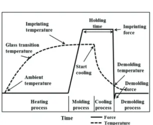
A thermal NIL is divided into four major steps: heating to imprinting temperature, isothermal molding by imprinting, cooling to demolding temperature with the force being maintained, demolding as shown Fig. 1. In the heating step, the polymer resist is heated above its glass transition
†E-mail: [email protected]
temperature (Tg). In the second step, the imprinting force is applied and held at a constant value for holding time. During this period, the mold moves closer to the substrate, the polymer resist flow into the mold cavity, and the residual layer is reduced. Upon the expiry of the molding, cooling starts while the imprinting force is maintained. Cooling is continued until the temperature of the molded part drops below the glass transition temperature or melting point of the polymer resist. When the demolding temperature of the polymer resist is reached, the molded part is demolded.
During the cooling and demolding process, it has been reported that fracture defects and deformations of the patterned part occurred mainly due to different thermal expansion rates and increased friction force between mold, polymer resist and substrate. Compare to the extensive researches on polymer deformation in the molding process [3-8], study on the cooling and demolding process is still lacking, even though several groups [9-13] have performed
Stress Analysis in Cooling Process for Thermal Nanoimprint Lithography with Imprinting Temperature and Residual Layer Thickness of Polymer Resist 69
Fig. 1. Typical process parameters related molding load and temperature during thermal NIL process.
exciting work.
In this paper, a cooling process of the polymer resist in thermal NIL is analyzed with finite element method. In this cooling temperature range, the polymer resist shows the viscoelastic behaviors with consideration of stress relaxation effect and time-temperature shift of the polymer. The modeling of cooling process for mold, polymer resist and substrate is developed. And the cooling process is numerically investigated with the effects of imprinting temperature and residual layer thickness of polymer resist on stress distribution of the polymer resist.
2. Numerical Analysis
2.1 Viscoelastic Behavior of the Polymer Resist The material behavior of thermoplastic polymer resists as a function of temperature is classified into three states as shown in Fig. 2. In the first region, where the temperature is below Tg, called the glassy state, the polymer resist can be assumed to be an elastic material. In the second region, where the temperature rises above Tg, called the rubbery state, the polymer resist’s viscosity steeply decreases with increasing temperature. In this state, the polymer resist displays dual responses of reversible and irreversible deformation to mechanical stresses, a property called viscoelasticity. Therefore, the polymer resist can be assumed to be a viscoelastic material in the rubbery state. As the temperature rises above the flow temperature (Tf), stress relaxation phenomena act quickly and irreversible deformation
Fig. 2. Typical deformation behavior of a thermoplastic polymer as a function of temperature.
becomes dominant. In this flow state, the polymer resist experiences fluid-like behaviors. In this paper, the temperature range of the simulation was set to be about Tg <
T < Tg + 70°C, so the polymer resist was assumed to be a viscoelastic material.
2.2 Governing and Constitutive Equations The governing and strain compatibility equation for the stress analysis of viscoelastic material is as follows:
, 0
ij j fi
σ +ρ = (1)
( , ,) 2
ij ui j uj i
ε = + (2)
where, σij, εij, fi are stresses, strains, and external forces.
Viscoelastic behavior is the time dependent response of a material to stress and strain. In the class of viscoelastic materials such as semi-molten state (rubbery state) polymer, the application of constant load is followed by a deformation, which can be made up of instantaneous deformation (elastic effect) followed by continual deformation with time (viscous effect), which results in the decay of the applied load and in termed as relaxation. Viscoelastic stress relaxation can be illustrated with mechanical elements, that is, springs and dashpots, where the spring represents the elastic behavior and dashpot represents viscous behavior.
The generalized Maxwell model was used to represent the stress relaxation behavior of the polymer during the thermal NIL process in this paper. In the stress relaxation form, the constitutive relation can be given by the following hereditary integral formulation:
Nam Woong Kim and Kug Weon Kim 70
( ) ( ) ( )
0
(0)
t
ij ijkl d kl ijkl kl
t G t d G t
d
σ τ ε τ ε
=∫ − τ + (3)
where the functions Gijkl(t) are called stress relaxation functions and t and τ represents current and past time respectively. The stress relaxation functions for materials with fading memory can be expressed in terms of Prony or exponential series.
( ) ( )
1
nexp
N
ijkl ijkl ijkl n
n
G t G ∞ G t λ
=
= +∑ − (4)
In the above, Gijkl∞is the equilibrium modulus at infinite time,
ijkln
G is the relaxation strength, λ is the relaxation n time and N is the total number of Prony series terms considered.
For the case of thermoelastic problems, under the assumption of thermo-rehelogically simple material, t and τ can be replaced by the reduced times t′ and τ′, which account for the superposition of time and temperature. The reduced time t′(T, t) is defined as the following equation:
( )
0
' t 1
T
t dt
=∫a t (5)
where the term aT is the shift factor of the time-temperature superposition principle. It is essentially a material property relating the response at a temperature T to the response function at the reference temperature To. In this paper, Williams-Landel-Ferry (WLF) equation was used as the shift function.
( ) ( )
( )
1 0
10
2 0
log a TT C T T
C T T
− −
= + − (6)
2.3 Material Property of the Polymer
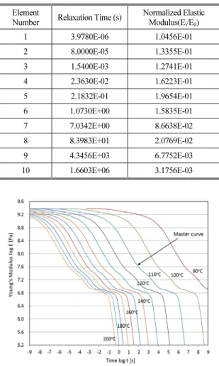
In this paper, we used the master stress relaxation functions of the polymer resist, Polymethyl Methacrylate (PMMA) that calculated 10-element Prony series coefficients by Song as shown in Table 1 [11]. E0 is 2.41GPa and Tg is considered as 110 °C. The coefficients of WLF equation C1 and C2 are 12.796 and 74.787 respectively.
Fig. 3 shows Young’s modulus of PMMA as a function of time and temperature under consideration of the time- temperature shift using the WLF equation.
Table 1. Elastic modulus and relaxation time for each Maxwell model in the simulation
Element
Number Relaxation Time (s) Normalized Elastic Modulus(Ei/E0)
1 3.9780E-06 1.0456E-01
2 8.0000E-05 1.3355E-01
3 1.5400E-03 1.2741E-01
4 2.3630E-02 1.6223E-01
5 2.1832E-01 1.9654E-01
6 1.0730E+00 1.5835E-01
7 7.0342E+00 8.6638E-02
8 8.3983E+01 2.0769E-02
9 4.3456E+03 6.7752E-03
10 1.6603E+06 3.1756E-03
Fig. 3. Young’s modulus of PMMA as a function of time and temperature using the WLF equation.
2.4 Finite Element Model
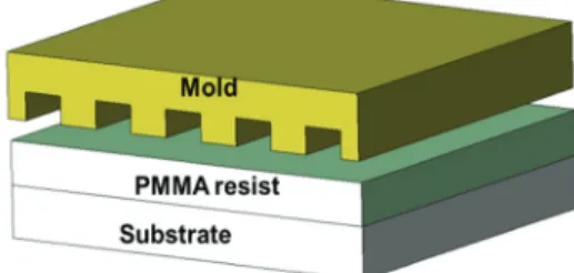
As countless many repeated nanometer scale patterns are defined on the mold, it is impractical to consider all of them in the analysis. If the cross sectional shape of mold is constant in one direction, that is line pattern, as shown in Fig.
4, two-dimensional analysis is possible. Moreover, if the offset and recess pattern of the mold is regular and symmetric, we can assume a two-dimensional plane strain model of a unit cell of the patterned mold as a finite element analysis model by taking repeated symmetric boundary conditions into account.
Fig. 5 shows a two-dimensional finite element model of mold/PMMA resist/substrate and boundary conditions are
Stress Analysis in Cooling Process for Thermal Nanoimprint Lithography with Imprinting Temperature and Residual Layer Thickness of Polymer Resist 71
shown. The depth of cavity area on the mold is 5µm and the aspect ratio of the feature is 1:2. Both the residual PMMA and the substrate have identical thickness of 5µm. The cavity area on the mold is fully occupied by PMMA resist.
The bottom surface is constrained on all three freedoms and a symmetric boundary condition is applied on left and right boundary. Since the PMMA resist is spin coated on substrate, the PMMA/substrate interface is defined as glued interface, no stress and displacement discontinuity is allowed; on the other hand, the interface between the mold and PMMA pattern is set to be slip-allowed, however, no penetration and separation on normal direction is allowed. These boundary conditions can be justified considering the fact that an anti- sticking coating is usually applied to the mold surface in order to reduce adhesion to the resist while increased adhesion is preferred between the PMMA resist and substrate. Uniform pressure of 10 MPa is applied on top surface of the stamp during the cooling process to compensate the thermal shrinkage during cooling and
Fig. 4. Schematic diagram of thermal NIL.
Fig. 5. Finite element model and boundary conditions of thermal NIL.
ensures the dimensional accuracy of replicated patterns. The analysis employs a commercial nonlinear finite element method code ABAQUS.
The material of the mold was silicon. Since silicon has a melting point of more than 1400 °C, it exhibits thermally strong characteristics at the process temperature used in the thermal NIL process. The properties of silicon used in the analysis are shown in Table 2.
Table 2. Material properties of silicon
Elastic Modulus [GPa] 128
Poisson Ratio 0.28
Thermal Expansion Coefficient [/oC] 2.5×10⁻⁶
3. Results & Discussion
Finite element method (FEM) simulations based on a 2-D symmetric model were performed to analyze the stress evolution and distribution of PMMA patterns for cooling step. The effects of imprinting temperature and residual layer thickness on the stress distribution of the PMMA resist pattern are investigated.
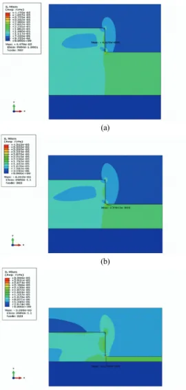
For the effects of imprinting temperature, five imprinting temperatures are considered, 200oC, 180oC, 160oC, 140oC, 120oC, and the demolding temperature is to be 40oC. Fig. 6 provides the relationship between imprinting temperature and maximum von Mises stress. Unlike the usual expec- tations, At lower imprinting temperature, the maximum von Mises stress appears to be higher, which is thought that the result may be due to the PMMA properties highly varying with temperature and complex stress distribution by different thermal expansion rates, and further research is needed. Fig. 7 shows the distribution of von Mises stress of PMMA pattern in cooling process from the imprint temperatures, 200oC, 160oC, 120oC, respectively. In all cases, the maximum von Mises stress occurs at the same position – the mold protrusion edge, which is in-line with studies reported earlier.
For the effects of residual layer thickness, the five layer thickness are considered, 1µm, 3µm, 5µm, 7µm, 9µm. The imprinting and the demolding temperature are to be 180oC, 40oC, respectively. Fig. 8 shows the relationship between residual layer thickness and maximum von Mises stress. The
Nam Woong Kim and Kug Weon Kim 72
Fig. 6. Maximum von Mises stresses with various imprinting temperatures.
(a)
(b)
(c)
Fig. 7. Distributions of von Mises stresses with various imprinting temperatures: (a) 200oC; (b) 160oC;
(c) 120oC.
Fig. 8. Maximum von Mises stresses with various residual layer thicknesses.
(a)
(b)
(c)
Fig. 9. Distributions of von Mises stresses with various residual layer thickness: (a) 9µm; (b) 5µm; (c) 1µm.
Stress Analysis in Cooling Process for Thermal Nanoimprint Lithography with Imprinting Temperature and Residual Layer Thickness of Polymer Resist 73
thicker the residual layer, the greater maximum von Mises stress. It can be seen that the residual layer thickness affects subsequent processes such as etching, but it also affects the generation of stress in the pattern layer during the cooling process. Therefore, care must be taken to ensure that the residual layer thickness is thin during molding process. Fig.
9 shows the distribution of von Mises stress of PMMA pattern with 9µm, 5µm, 1µm residual layer thickness respectively. In all cases, the distribution of von Mises stress is very similar.
4. Conclusions
The following conclusions can be drawn.
1. With the consideration of a viscoelasticity for the polymer resist in cooling temperature range for thermal NIL, an analysis modeling for cooling process is developed. The main features of the analysis model are as follows: a two- dimensional plane strain model of a unit cell of the line patterned mold, glued interface between polymer resist and substrate, slip-allowed interface between polymer resist and mold.
2. To investigate the effects of imprinting temperature on stress distribution during cooling, five imprinting tem- peratures are considered, 200oC, 180oC, 160oC, 140oC, 120oC. The analysis results show that at lower imprinting temperature, the maximum von Mises stress appears to be higher, which may be due to the polymer properties highly varying with temperature and complex stress distribution by different thermal expansion rates.
3. For the effects of residual layer thickness on stress distribution during cooling, the five layer thickness are considered, 1µm, 3µm, 5µm, 7µm, 9µm. The analysis results show that the thicker the residual layer, the greater maximum von Mises stress. As the residual layer thickness also affects subsequent processes such as etching, care should be taken to ensure that the residual layer thickness is thin during molding process.
Acknowledgement
This work was supported by the Soonchunhyang University Research Fund.
References
1. Chou, S. and Krauss, P., “Imprint lithography with sub10 nm feature size and high throughput,” Microe- lectronic Engineering, Vol. 35, pp. 237-240, (1997).
2. Guo, L. J. “Recent progess in nanoimprint technology and its applications,” Journal of Physics D: Applied Physics, Vol.37, pp. R123-R142, (2004).
3. Hirai, Y., Konish, T., Yoshikawa, T. and Yoshida, S.,
“Simulation and Experimental Study of Polymer Deformation in Nanoimprint Lithography,” J. Vac. Sci.
Technol. B, Vol. 22, pp. 3288-3293, (2004).
4. Kim, N.W., Kim, K.W. and Sin, H.-C., “A Viscoelasitc Finite Element Analysis of Thermal Nanoimprint Lithography Process,” Journal of the Microelectronics
& Packaging Society, Vol. 14, No. 4, pp. 1-7, (2007).
5. Kim, N.W., Kim, K.W. and Sin, H.-C., “Effect of Pressure and Initial Polymer Resist Thickness on Low Temperature Nanoimprint Lithography,” Journal of manufacturing engineering & technology, Vol. 18, No. 1, pp. 68-75, (2009).
6. Kim, N.W., Kim, K.W. and Sin, H.-C., “Finite element analysis of low temperature thermal nanoimprint lithography using a viscoelastic model,” Micro- electronic Engineering, Vol. 85, pp. 1858-1865, (2008).
7. Lee, K.Y. and Kim, K.W., “A Study on the Filling Process and Residual Layer Formation in Nanoimprint Lithography Process,” Journal of the Korea Academia- Industrial Cooperation Society, Vol. 13, No. 9, pp. 3835- 3840, (2012).
8. Lee, K.Y. and Kim, K.W., “Numerical Analysis of Pressure and Temperature Effects on Residual Layer Formation in Thermal Nanoimprint Lithography,”
Journal of the Semiconductor & Display Equipment Technology, Vol. 12, No. 2, pp. 93-98, (2013).
9. Hirai, Y., Yoshida, S. and Takagi, N., “Defect Analysis in Thermal Nanoimprint Lithography,” J. Vac. Sci.
Technol. B, Vol. 21, pp. 2765-2770, (2003).
10. Worgull, M., Heckele, M., Hétu, J. F., and Kabanemi, K.
K., “Modeling and optimization of the hot embossing process for micro and nanocomponent fabrication,” J.
Microlith. Microfab. Microsyst., Vol. 5, No. 1, pp.
011005/1-13, (2006).
Nam Woong Kim and Kug Weon Kim 74
11. Song, Z., “Study of Demolding Process in Thermal Imprint Lithography via Numerical Simulation and Experimental Approaches,” M.S. Thesis, Louisiana State University, (2007).
12. Dirckx, M. E., “Demolding of Hot Embossed Polymer Microstructures,” Ph. D. Thesis, MIT, (2010).
13. Omar, F., “Hot Embossing Process Parameters:
Simulation and Experimental Studies,” Ph. D. Thesis, Cardiff University, (2013).
접수일: 2017년 12월 11일, 심사일: 2017년 12월 23일, 게재확정일: 2017년 12월 26일