• 검색 결과가 없습니다.

Photoelectrochemical Hydrogen Production on Textured Silicon Photocathode

N/A
N/A
Protected

Academic year: 2021

Share "Photoelectrochemical Hydrogen Production on Textured Silicon Photocathode"

Copied!
5
0
0

로드 중.... (전체 텍스트 보기)

전체 글

(1)

Vol. 14, No. 4, 2011, 191-195 DOI:10.5229/JKES.2011.14.4.191

− 191 −

Photoelectrochemical Hydrogen Production on Textured Silicon Photocathode

Ilwhan Oh*

Korea Advanced Nanofabrication Center, Suwon, Gyeonggi 444-270 (Received October 19, 2011 : Accepted October 24, 2011)

Abstract : Wet chemical etching methods were utilized to conduct Si surface texturing, which could enhance photoelectrochemical hydrogen generation rate. Two different etching methods tested, which were anisotropic metal-catalyzed electroless etching and isotropic etching. The Si nano-texture that was fabricated by the anisotropic etching showed ~25% increase in photo- current for H2 generation. The photocurrent enhancement was attributed to the reduced reflec- tion loss at the nano-textured Si surface, which provided a layer of intermediate density between water and the Si substrate.

Keywords : Silicon texturing, Metal-catalyzed electroless etching, Photoelectrochemistry, Hydrogen evolution reaction, Solar water splitting

1. Introduction

Recently a renewed interest has been shown in solar water splitting as a potential solution to provide emission- free clean hydrogen fuel for transportation and other energy applications.

1)

Photoelectrochemical hydrogen production at the semiconductor/electrolyte interface has been studied for decades.

2-4)

In solar fuel production, a photoelectrochemical cell converts photon energy into chemical energy and generates H

2

on cathode and O

2

on anode, as described in the following half-cell reactions:

2H

+

+ 2e

→ H

2

(cathode) (1a)

H

2

O → 1/2 O

2

+ 2H

+

+ 2e

(anode) (1b) The Gibbs free energy change ∆ G

o

of the net reaction is 237 kJ/mol, or equivalently, the standard emf ∆ E

o

is − 1.23 V. As the negative emf indicates, the net reaction is energetically uphill reaction.

Silicon is earth-abundant, relatively low-cost semicon- ductor material that is most widely used in current photovoltaics, with vast knowledge base and infrastruc- ture.

5)

The photoelectrochemical H

2

generation at the

Si/electrolyte interface has been studied for decades.

6-10)

Compared to the solid-state solar conversion devices, one of the disadvantages of the solar energy conversion devices based on semiconductor/electrolyte interface is that it very difficult or impossible to introduce anti- reflection layer (e.g., SiO

2

and/or Si

x

N

y

coating on top of the p-n junction in the conventional Si solar cells), because such layer will easily block the electron transfer at the semiconductor/electrolyte interface. As depicted in Fig. 1, due to the large difference in the refractive indices of Si (n = 3.5) and electrolyte (n = 1.3), the planar Si/electrolyte interface reflects as much as 25% of the incident visible light.

11)

Alternative approach to reduce

*E-mail: ioh0204@gmail.com

Fig. 1. (A) Schematic showing reflection loss at the

semiconductor/electrolyte interface which has a large

difference in refractive indexes values (n). (B) Surface texturing

can reduce reflection at the semiconductor/electrolyte interface

by providing an anti-reflection layer with intermediate

density between water and the Si substrate.

(2)

the reflection loss is Si surface texturing. Surface texturing usually refers to introducing micrometer or even nanometer scale embossing structures on the Si surface, which effectively reduces reflection loss of incident photon thus enhances generated photocurrent.

12-14)

Fabrica- tion methods for the Si surface texturing includes alkaline etch, acid etch, and reactive ion etch (RIE). The RIE method requires expensive and cumbersome ultra-high vacuum equipments. On the other hand, wet chemical processes provide a simple, rapid, and effective route to low-reflectance Si surface texturing. Among several different wet etch systems, the HF/HNO

3

system is the most commonly used low-temperature process. In spite of the direct benefit that can be obtained from the surface texturing, adoption of the surface texturing into the semiconductor/electrolyte interface has been rarely investigated.

11)

Here in this work, we utilized two different room- temperature wet etch methods for Si surface texturing:

the HF/HNO

3

system and the metal-catalyzed HF etching.

Optical and electron microscopy measurements showed that the wet etch methods effectively produced micrometer- or nanometer-sized pits/pores or grooves on the Si surface. The textured Si surface was evaluated by measuring the photoelectrochemical H

2

generation.

Effect of the surface texturing on the magnitude of photocurrent was examined and discussed.

2. Experimental

2.1. Wet chemical texturing of crystalline Si A p-type Si (100) wafer (Wafer World, Inc.; ~10 ohm- cm; B-doped) was degreased by rinsing with acetone, isopropyl alcohol, and ultrapure deionized water (DIW) in sequence. The Si surface was further cleaned by immersing in piranha (1 : 3 H

2

O

2

+ H

2

SO

4

) for 3 min and in 1 : 10 HF for 2 min to remove surface oxide.

Backside ohmic contact was formed by depositing and annealing an ohmic metal layer onto the HF-treated Si wafer. For metal-catalyzed electroless etching, the Si sample was immersed in 8 mM AgNO

3

and 4.6 M HF for a designated duration of time, then transferred to diluted HNO

3

to remove dendritic Ag residue. For isotropic etching, the cleaned Si sample was immersed in a 1 : 1 (v/v) mixture of 60% HNO

3

and 50% HF for a designated duration of time, then thoroughly rinsed with deionized water.

2.2. Photoelectrochemical H

2

generation measure- ments

For photoelectrochemical measurements, a O-ring sealed Teflon cell was used that could accommodate a three-electrode configuration and secure a light path to the Si/electrolyte interface. Backside ohmic metal was electrically connected to a Cu metal foil. The front side of the Si sample was firmly pressed and sealed with a Teflon O-ring, by which the projected electrode area was defined. (0.286 cm

2

) A Pt counter electrode and a standard calomel reference electrode (SCE) were used.

For illumination source, a halogen lamp was used, the intensity of which was controlled by the distance between the lamp and the photoelectrochemical cell. A Si photodiode (Hamamatus; model S2386-18K) was used for intensity calibration. All glassware was thoroughly cleaned in an oxidizing bath (Nochromix, Godax Laboratories, Inc.) and rinsed with ultrapure water prior to use. Electrolyte solution was prepared by adding concentrated H

2

SO

4

(Aldrich) into 0.5 M K

2

SO

4

along with pH measurement. All chemicals were used as received. All measurements were conducted in three- electrode configuration using a CHI 660D potentiostat.

3. Results and Discussion

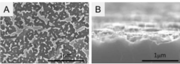
Fig. 2 shows SEM micrographs of the textured Si, which was fabricated by metal-catalyzed electroless etching (MCEE) of bulk crystalline p-type (100)-Si (10 W-cm; B-doped) in 8 mM AgNO

3

and 4.6 M HF for 6 min. In the MCEE method, oxidizing agent (Ag

+

in current work) provides holes that are needed to oxidize Si atoms and, at the same time, HF etches away Si atoms.

15-20)

Etchant composition of the MCEE method

Fig. 2. Scanning electron micrographs of the surface nano- textured Si, which was fabricated by metal-catalyzed electroless etching (MCEE) of bulk crystalline p-type (100)-Si (10 W- cm; B-doped) in 8 mM AgNO

3

and 4.6 M HF for 6 min.

(A) Top view of the nano-textured Si surface showing. (B)

Profile view of the nano-textured Si layer.

(3)

is similar to the traditional Si etchants in the sense that both oxidizing agent and HF are present. However, Ag

+

is reduced to form nanostructured deposit on the Si surface, which functions as nanostructured template in the further etching of the underlying Si. As shown in Fig. 2(A), the Si surface textured through the MCEE method exhibits nano-texture that ranges from 50 to 200 nm in lateral dimension. Cross-sectional image in Fig. 2(B) shows that the vertical dimension of the nano- texture is ~200 nm. The vertical dimension is increased in proportion to etch time. Because the dimension of the nano-texture is comparable to the wavelength of visible light, the nano-textured surface effectively suppresses light reflection at the surface, which is evidenced by

‘black’ surface color with low reflection as compared to mirror-like surface of polished planar Si.

Fig. 3 shows an optical microscope image of the Si surface, which was textured by isotropic etching of the same crystalline Si in a 1 : 1 (v/v) mixture of 60%

HNO

3

and 50% HF for 10 sec.

The HNO

3

/HF etch system is the most commonly used isotropic Si etchant composition. Because the HNO

3

/ HF etch system is an isotropic etchant, the image in Fig. 3 exhibits macroscopic grooves tens of microns in lateral dimension, in contrast to the nano-textured features produced by the MCEE method in Fig. 2.

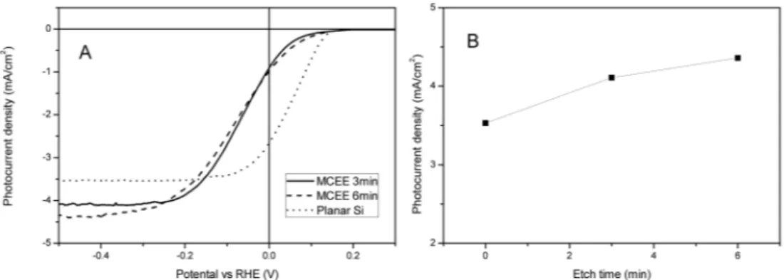
Fig. 4 shows photoelectrochemical measurements of the Si photocathodes, which were textured by the MCEE method, in acidic solution of H

2

SO

4

+ 0.5 M K

2

SO

4

(pH 1). During the measurements, the textured Si photocathode was constantly illuminated with simulated sunlight (intensity = 16mW/cm

2

). When the Si photo- cathode absorbs a photon, a minority carrier (electron in case of p-type Si) is generated and flows toward the semiconductor/electrolyte interface, where the minority carrier is transferred across the semiconductor/electrolyte interface, reducing H

+

to H

2

. Fig. 4(A) shows the current density (J)-electrode potential (E) measurements on the textured Si photocathode. When E is more positive of 0.2 V, the value of J is virtually zero and H

2

is not produced. As E is scanned in negative direction, the current increases and, at the potential regime more negative of − 0.2 V, reaches a limiting photocurrent that is determined mainly by the transmitted photon intensity.

The sigmoidal J-E graph is typical of photon-limited photoelectrochemical response. In Fig. 4(A), the MCEE- textured Si photocathodes exhibits enhanced photocurrent compared to the planar Si. This result indicates that,

Fig. 4. (A) Photoelectrochemical H

2

generation on MCEE Si photocathode in a solution of H

2

SO

4

+ 0.5 M K

2

SO

4

(pH 1) with simulated solar radiation (intensity = 16 mW/cm

2

). The Si surface is textured by metal-catalyzed electroless etching in 8 mM AgNO

3

and 4.6M HF for a designated time (B) Relationship between limiting photocurrent and electroless etch time.

Fig. 3. Optical microscope image the Si surface, which

was textured by isotropic etching of crystalline p-type

Si(100) (resistivity ~10 W-cm; B-doped) in a 1 : 1 (v/v)

mixture of 60% HNO

3

and 50% HF for 10 sec.

(4)

while substantial amount of incident photon is reflected at the mirror-like planar Si interface, the textured Si surface significantly reduces reflection loss and generates larger current. Fig. 4(B) shows the effect of etch time on the limiting photocurrent density. Compared to the planar Si (etch time = 0 min), the 6-min electroless etched Si photocathode shows as large as 24% increase in photocurrent. Previous report indicates that, at the mirror-like planar Si/electrolyte interface, as large as 25%

of the incident solar radiation is reflected.

11)

On the other hand, the nano-textured Si surface provides an anti- reflection layer with intermediate density and refractive index between water and the Si substrate, dramatically reducing reflection at the Si interface.

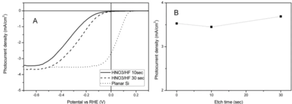
Fig. 5 shows photoelectrochemical measurements of the Si photocathodes, which were textured by the HNO

3

/ HF isotropic etchant, in acidic solution of H

2

SO

4

+ 0.5M K

2

SO

4

(pH 1) illuminated with simulated sunlight (intensity = 16 mW/cm

2

). Comparison of limiting photocurrents indicates that the isotropic etching of Si provides little enhancement. This result indicates that the macroscopic grooving produced from the isotropic etching, as observed in Fig. 3, is not very effective in reducing light reflection from the Si surface. Furthermore, after the isotropic etching, the photovoltage is significantly reduced, indicating formation of passivation layer or change of surface chemistry at the etched Si surface.

4. Conclusion

Two different wet chemical etching methods were

evaluate for Si surface texturing to reduce reflection loss at the Si/electrolyte interface: the anisotropic etching assisted by metal ion and the isotropic etching in the HNO

3

/HF system. Optical and electron microscopy measurements verifies that the MCEE method produces a nano-textured surface that functions as effective anti- reflection layer by providing intermediate density layer between water and the Si substrate, while the isotropic etching produces macroscopic grooves on the Si surface.

Photoelectrochemical H

2

generation measurements showed that the anisotropic etched Si photocathode exhibited

~25% enhancement in photocurrent, which was attributed to reduced light reflection at the nano-textured Si interface.

References

1. J. A. Turner, ‘Sustainable Hydrogen Production’, Science, 305, 972, (2004).

2. A. Heller, ‘Conversion of sunlight into electrical power and photoassisted electrolysis of water in photoelectro- chemical cells’, Acc. Chem. Res., 14, 154, (1981).

3. M. G. Walter, E. L. Warren, J. R. McKone, S. W. Boettcher, Q. Mi, E. A. Santori, and N. S. Lewis, ‘Solar Water Splitting Cells’, Chem. Rev., 110, 6446, (2010).

4. A. J. Bard and M. A. Fox, ‘Artificial Photosynthesis:

Solar Splitting of Water to Hydrogen and Oxygen’, Acc.

Chem. Res., 28, 141, (1995).

5. A. Luque and S. Hegedus, Eds., Handbook of photovoltaic science and engineering, John Wiley & Sons, West Sussex, (2003).

6. D. C. Bookbinder, N. S. Lewis, M. G. Bradley, A. B.

Bocarsly, and M. S. Wrighton, ‘Photoelectrochemical

reduction of N,N´-dimethyl-4,4´-bipyridinium in aqueous

Fig. 5. (A) Photoelectrochemical H

2

generation on Si photocathode in a solution of H

2

SO

4

+ 0.5 M K

2

SO

4

(pH 1) with

simulated solar radiation (intensity = 16 mW/cm

2

). The Si surface is textured by isotropic etching in a 1 : 1 (v/v) mixture

of 60% HNO

3

and 50% HF for a designated time (B) Relationship between limiting photocurrent and etch time.

(5)

media at p-type silicon: sustained photogeneration of a species capable of evolving hydrogen’, J. Am. Chem.

Soc., 101, 7721, (1979).

7. A. B. Bocarsly, D. C. Bookbinder, R. N. Dominey, N. S.

Lewis, and M. S. Wrighton, ‘Photoreduction at illuminated p-type semiconducting silicon photoelectrodes. Evidence for fermi level pinning’, J. Am. Chem. Soc., 102, 3683, (1980).

8. D. C. Bookbinder, J. A. Bruce, R. N. Dominey, N. S. Lewis, and M. S. Wrighton, ‘Synthesis and characterization of a photosensitive interface for hydrogen generation: Chemi- cally modified p-type semiconducting photocathodes’, Proc. Nat. Acad. Sci., 77, 6280, (1980).

9. Y. Nakato, Y. Egi, M. Hiramoto, and H. Tsubomura,

‘Hydrogen evolution and iodine reduction on an illuminated n-p junction silicon electrode and its application to efficient solar photoelectrolysis of hydrogen iodide’, J. Phys.

Chem., 88, 4218, (1984).

10. S. W. Boettcher, J. M. Spurgeon, M. C. Putnam, E. L.

Warren, D. B. Turner-Evans, M. D. Kelzenberg, J. R.

Maiolo, H. A. Atwater, and N. S. Lewis, ‘Energy- conversion properties of vapor-liquid-solid-grown silicon wire-array photocathodes’, Science, 327, 185, (2010).

11. J. Oh, T. G. Deutsch, H.-C. Yuan, and H. M. Branz,

‘Nanoporous black silicon photocathode for H2 production by photoelectrochemical water splitting’, Ener. Env. Sci., 4, 1690, (2011).

12. P. Campbell and M. A. Green, ‘Light trapping properties of pyramidally textured surfaces’, J. App. Phys., 62, 243, (1987).

13. B. Gonzalez-Diaz, R. Guerrero-Lemus, B. Diaz-Herrera,

N. Marrero, J. Mendez-Ramos, and D. Borchert,

‘Optimization of roughness, reflectance and photolumines- cence for acid textured mc-Si solar cells etched at different HF/HNO

3

concentrations’, Mat. Sci. Eng.: B, 159-160, 295, (2009).

14. K. Kim, S. K. Dhungel, S. Jung, D. Mangalaraj, and J. Yi,

‘Texturing of large area multi-crystalline silicon wafers through different chemical approaches for solar cell fabrication’, Sol. Ener. Mat. Sol. Cells, 92, 960, (2008).

15. A. I. Hochbaum, R. Chen, R. D. Delgado, W. Liang, E. C. Garnett, M. Najarian, A. Majumdar, and P. Yang,

‘Enhanced thermoelectric performance of rough silicon nanowires’, Nature, 451, 163, (2008).

16. A. I. Hochbaum, D. Gargas, Y. J. Hwang, and P. Yang,

‘Single Crystalline Mesoporous Silicon Nanowires’, Nano Lett., 9, 3550, (2009).

17. K.-Q. Peng, Y.-J. Yan, S.-P. Gao, and J. Zhu, ‘Synthesis of Large-Area Silicon Nanowire Arrays via Self-Assembling Nanoelectrochemistry’, Adv. Mat., 14, 1164, (2002).

18. Y. Qu, L. Liao, Y. Li, H. Zhang, Y. Huang, and X. Duan,

‘Electrically Conductive and Optically Active Porous Silicon Nanowires’, Nano Lett., 9, 4539, (2009).

19. M.-L. Zhang, K.-Q. Peng, X. Fan, J.-S. Jie, R.-Q. Zhang, S.-T. Lee, and N.-B. Wong, ‘Preparation of Large-Area Uniform Silicon Nanowires Arrays through Metal-Assisted Chemical Etching’, J.Phys. Chem. C, 112, 4444, (2008).

20. X. Zhong, Y. Qu, Y.-C. Lin, L. Liao, and X. Duan,

‘Unveiling the Formation Pathway of Single Crystalline

Porous Silicon Nanowires’, ACS App. Mat. Inter., 3, 261,

(2011).

수치

Fig. 1. (A) Schematic showing reflection loss at the semiconductor/electrolyte interface which has a large difference in refractive indexes values (n)
Fig. 2 shows SEM micrographs of the textured Si, which was fabricated by metal-catalyzed electroless etching (MCEE) of bulk crystalline p-type (100)-Si (10 W-cm; B-doped) in 8 mM AgNO 3  and 4.6 M HF for 6 min
Fig. 4 shows photoelectrochemical measurements of the Si photocathodes, which were textured by the MCEE method, in acidic solution of H 2 SO 4 + 0.5 M K 2 SO 4  (pH 1)
Fig. 5 shows photoelectrochemical measurements of the Si photocathodes, which were textured by the HNO 3 / HF isotropic etchant, in acidic solution of H 2 SO 4 + 0.5M K 2 SO 4  (pH 1) illuminated with simulated sunlight (intensity = 16 mW/cm 2 )

참조

관련 문서

In the hydrogen production by steam reforming of LNG, the catalytic performance of NA and M/NA catalysts was well correlated with the nickel surface area of the

1. Prismless layer was commonly observed on the fissure enamel in young and mature premolar. There were no differences in micro-structure and etching

Discontinuum Continuum.. and Min, K.B., 2015, Discrete element modeling of transversely isotropic rock applied to foundation and borehole problems, 13 rd ISRM

Photoluminescence properties and surface morphologies of porous silicon were investigated by controlling of etching times and applied current densities..

K., "Hydrogen production by catalytic decomposition of methane over activated carbons: kinetic study", International Journal of Hydrogen Energy, Vol...

Plasma는 강한 산화/환원성을 가진 재료로 구성되며 일정 압력 하에서 다양한 방법으로 가해지는 전계(Electric Field)에 의해 기체 상태로 가속된 입자가 되어 식각 대상 재료와 만날

Recently, metal-assisted chemical etching (MACE) has been widely used for the synthesis of SiNWs, because this technique has advantages such as simplicity, low operating

J., “Hydrogen production from partial oxidation of dimethyl ether using corona discharge plasma”, International Journal of Hydrogen Energy , Vol.. Liu C.,