한국산업정보학회논문지 제16권 제5호(2011. 12)
Minimal Leakage Pattern Generator †
Kyung Ki Kim
*Abstract This paper proposes a new input pattern generator for minimal leakage power in the nanometer CMOS technology considering all the leakage current components (sub-threshold leakage, gate tunneling leakage, band-to-band tunneling leakage). Using the accurate macro-model, a heuristic algorithm is developed to generate a input pattern for the minimum leakage. The algorithm applies to ISCAS85 benchmark circuits, and the results are compared with the results of Hspice. The simulation result shows that our method's accuracy is within a 5% difference of the Hspice simulation results. In addition, the simulation time of our method is far faster than that of the Hspice simulation.
Key Words : Direct Input Output Manufacturing System(DIOMS), Genetic Algorithm
1. Introduction
As MOSFET technology is scaled down more aggressively, leakage power has become more and more significant in power dissipation because of the continued scaling of supply voltage and threshold voltage (V
th). In nanometer CMOS circuits, the main leakage components are sub-threshold, gate tunneling, and reverse biased junction band-to-band- tunneling (BTBT) leakage current.
As transistor geometries are reduced, it is necessary to reduce the supply voltage to avoid electrical break down and to obtain the required performance. However, to retain or improve performance, it is necessary to reduce the threshold voltage (V
th) as well, which results in exponential increase of sub-threshold leakage. To control short channel effect and increase the transistor driving strength in deep sub-micron circuits, gate-oxide thickness also becomes thinner as technology scales
* Assistant Professor, School of Electronic Engineering, Daegu University, South Korea, Corresponding Author (e-mail:
kkkim@daegu.ac.kr)
down. The aggressive scaling in the gate-oxide results in tunneling current through the oxide, which is a strong exponential function of the oxide thickness and the voltage magnitude across the oxide. In scaled devices, the higher substrate doping density and the application of the ”"halo”" profiles cause significantly large reverse biased junction band-to-band-tunneling (BTBT) leakage current through drain- substrate and source-substrate junctions [1]- [3].
This problem is very serious in portable electronic systems that operate mostly in sleep mode. In order to minimize the leakage power dissipation, several circuit techniques have been proposed such as power gating structure, and variable threshold voltage CMOS using variable substrate bias voltage.
However, these techniques require significant circuit modifica- tion and performance overhead for leakage reduction[3].
Another technique with little or no overhead is
the input pattern control technique based on stack
effect: the amount of leakage currents of nanometer
CMOS circuit varies depending on the input pattern.
However, it is an NP-hard problem to determine the input pattern that sets up the minimum leakage current during standby mode without any hardware overhead or architecture change. Several techniques have been proposed to generate the minimum leakage test pattern and solve the NP-hard problem [4]-[7]. None of these techniques explicitly considers the interactions among the sub-threshold leakage, gate tunneling leakage, and BTBT leakage.
Moreover, better understanding and more accurate model of leakage currents are required for the input pattern control in the nanometer CMOS circuits.
In this paper, all the possible leakage current components are investigated, and a novel macro-modeling technique is proposed to characterize the minimum leakage current of each individual leaf cell considering the interaction among all the leakage components. A heuristic approach is developed in order to find the input pattern for minimum leakage current during standby mode of nanoscale VLSI chips. Finally, a simple circuit is proposed to the low-leakage input pattern can be applied to a real circuit during standby mode. The proposed approach uses the functional dependencies in the VLSI and the controllability of its nodes.
2. Leakage Power
A transistor switch is essentially a resistive -capacitive network between the power supply and ground. Due to the non-ideal off-state characteristics (a finite resistance) of a tran- sistor, current is drawn from the power supply even when a transistor operates in the cutoff region. The leakage currents are dominated by weak inversion and reverse biased p-n junction diode currents in long channel devices [3]. In nanometer integrated circuits, other leakage mechanisms such as gate oxide tunneling and junction band-to-band-tunneling
(BTBT) are also important [2][3]. In off-state, the main components of leakage current are sub- threshold leakage (I
sub), gate-induced drain leakage (I
GIDL), gate tunneling leakage (I
gate), and band-to-band tunneling (I
BTBT) as shown in Fig. 1 (a). Gate tunneling leakage (Igate) is the major component during on-state as shown in Fig. 1 (b).
(a)
(b)
<Figure 1> Leakage current in nanoscale CMOS circuit: (a) Off-state leakage compo- nents, (b) On-state leakage components.
The GIDL (Gate Induced Drain Leakage) is a
current from drain to sub-strate caused by high
electric field between gate and drain, and thin gate
oxide thickness and high supply voltage increase
the GIDL leakage. The gate tunneling leakage is the
current flowing into the gate of the transistor by
tunneling effect, and thin gate oxide thickness and
high supply voltage increase the gate tunneling
leakage. The sub-threshold leakage is the weak inver- sion conduction current of the CMOS transistor when V
gsis less than V
th. It increases exponentially due to the reduced threshold voltage, and it is a main leakage component in high forward body bias case. Finally, the BTBT leakage is the current by electron tunneling across the reverse biased p-n junction between drain/source and subs- trate of the CMOS transistor.
Therefore, in high reverse body bias case, the BTBT leakage becomes a major portion of the total leakage currents. The sub-threshold leakage current and the BTBT leakage are much more sensitive to the applied body bias than other two leakage components. The minimum leakage current is obtained when the sub-threshold leakage current is equal to the BTBT leakage.
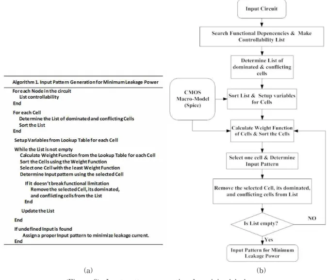
3. Input Pattern Generation
Based on the fan-out effect in leakage current, the macromodel for a leaf cell (inverter, NAND, and NOR gates) is developed based on an Hspice simulation, where the controlling variables are the number of fan-outs, the cell size, and the input pattern, considering the stack effect under fixed VDD, V
th, t
ox, and temperature. On the basis of the accurate macromodel of the cells, a heuristic approach is implemented to generate the minimum leakage test pattern. The leakage of each cell in the circuit depends on the input pattern applied to the circuits. Researchers have proposed several techniques to generate the input pattern for minimum leakage current and solve the NP-hard problem [4]-[7]. An easy way to solve the problem is to use the functional dependencies in the circuits and the controllability of the nodes. In this research, the methodology is improved to estimate the accurate leakage current with a fast simulation time.
The functionality of the cells in circuits determines the states of the internal nodes for any given input vector. A cell is "dominated" if its input pattern causing the minimum leakage current is a subset of the minimum leakage input pattern of the other cells.
A cell is "conflicting" if the input pattern causing the minimum leakage conflicts with other cells input vectors that cause the minimum leakage. Before finding the optimal input pattern to reduce leakage power dissipation, the func- tional dependencies between cells should be searched, and each cell's dominated and conflicting cells should be listed in the order of the weight function, which is given by
c cc dc
fG
( ) ( ( )) ( ( ))
( )
i i i
i i
i
W G MLK G MLK G MLK MLK G
= -
- -
å å
(1)
where W
c(G
i) is the weight of cells G
i. MLK
cc, MLK
dc, and MLK
fGare the mean leakage for conflicting cells, dominating cells, and fan-out of G
i, respectively.
Once the list is determined, the cell that has the least weight function will be selected. If the cell satisfies the functional constraints for minimum leakage current, the PI patterns controlled by the cell are determined. After finding the proper input patterns, the cell is removed from the list, and at the same time the cell's dominated and conflicting cells are removed. This procedure is repeated until there are no cells in the list or only undefined cells remain. If the undefined cells are found, proper patterns must be assigned, considering the conditions for low leakage current, because these cells have no dominated or conflicting cells.
An example circuit shown in Fig. 2 explains this
proposed heuristic approach in detail. As described at
the beginning of this subsection, a macromodel is
generated for all the cells in the library, and the
macrocells contain all the leakage current information
for all the possible input and fan-out cases.
For example, the two -input NAND gate and the two-input NOR gate in Fig. 2 have the leakage currents shown in Table 1 and Table 2 for different inputs and a fan-out of 2, respectively.
<Figure 2> Example circuit, which is used as an example to explain the proposed heuristic algorithm.
<Table 1> Leakage currents for a NAND.
Input1 Input2 Total Leakage Current
0 0 21.5
nA
0 1 40.8
nA
1 0 18.0
nA
1 1 186.0
nA
<Table 2> Leakage currents for a NOR.
Input1 Input2 Total Leakage Current
0 0 38.6 nA
0 1 58.9 nA
1 0 46.5 nA
1 1 73.9 nA
In Table 1, Input1 represents the input to the transistor closest to the output. For a NAND gate, the total leakage is the lowest when the inputs are (1, 0) and the gate leakage current is dominant over the sub-threshold current. If the sub-threshold current is larger than the gate leakage, then the total leakage is lowest when the inputs are (0, 0).
In this research, it is considered that nanoscale CMOS technology has a larger gate-tunneling
current than the sub-threshold current. The primary-input patterns for minimum leakage current and the lists of dominating and conflicting cells are created using the test controllability lists of the example circuit. The possible input patterns can be obtained from the macromodel of each cell.
<Table 3> Input pattern for minimal leakage.
Cell Minimum leakage input pattern of
each cell
Minimum leakage input
pattern
Conflicting cells Input 1 Input 2 A1 A2 A3 A4
G1 1 0 1 0 X X G4, G5, G6
G2 1 0 X 0 0 X G4, G6, G6
G3 1 0 X X 0 0 G4, G5, G6
G4 0 0 1 1 1 X G1, G2, G3
G5 0 0 X 1 1 1 G1, G2, G3
G6 1 0 1 1 1 0 G1, G2, G3
The detailed procedure is as follows: On the basis of the leakage current information of each cell from the macromodel and the controllability for the example circuit, PI patterns that minimize leakage current are generated, then the conflicting and dominated cell lists are identified, as Table 3 shows.
Based on the leakage information of a two-input NAND gate and a two-input NOR gate shown in Table 1 and Table 2, the input patterns of the example circuit for minimal leakage power dissipation are generated. The whole algorithm is summarized in Fig. 3.
The generated input patterns are "1000" and
"0001" which make the circuit dissipate the minimal
leakage power of 22.3 nW. On the other hand, an
maximal leakage input pattern, "1111" makes the
circuit dissipate 125 nW. Therefore, the minimal
leakage pattern can give around 6x reduction in
leakage power dissipation.
(a) (b)
<Figure 3> Input pattern generation for minimal leakage:
(a) Pseudo-code the proposed algorithm, (b) Overall flow of the proposed method 4. Data Retention Circuit
A simple circuit should be added to each latch such that the low-leakage input vector (found by
the proposed approach) can be applied to a combinational circuit during standby mode. As a solution, pass-gate multiplexors and NAND/NOR gates can be used to force the inputs of the combinational logic circuits to the desired value during the sleep mode. However, since the combinational circuit being analyzed is assumed to be part of sequential network, the latches in the
sequen- tial network can be easily modified to force either a 0 or 1 during the sleep mode.
Figure 4 shows standard static latches that have been modified to force a desired value at the input
of the combinational circuit during the sleep mode.
The modified latch requires a small modification of
the design; this is in line with current practice as
used for most functional units in pipelined data
paths. The signal that enables a unit, can be used
to activate the input latches, thus providing
recovery within one clock period and causing no
performance overhead in most cases.
However, the circuit topology should be used in the sequential network because if units without the latches require the addition of the latches for low-leakage input vector control, the actual power consumption increases, and the area overhead becomes noticeable. Clearly, other types of latches and flip-flops can also be modified in similar ways to force appropriate values during the sleep mode.
In the sequential network, the data retention circuit has little speed and area overhead.
(a)
(b)
<Figure 4> Data retention circuit with a latch:
(a) For high-level, (b) For low-level.
As an example, Fig. 5 shows the ISCAS85 C17 benchmark circuit using the data retention circuit.
In Fig. 5, the "High" block is a data retention circuit for the logic HIGH ("1") level, and the
"Low" block is a data retention circuit for the logic LOW ("0") level. The clock signals of each latch are controlled by the two clock gating circuits. If the sleep signal is "ON", the primary inputs of the
C17 circuit are set to the minimal leakage input vector. Then, the simple clock gating circuit (without the flip-flop) in Fig. 5 is activated; the clock signal of each latch remains in the "LOW"
state, and data (placed prior to the sleep mode) is saved on each latch. If the sleep signal is "OFF", then the data retention circuit and the clock gating are not activated and the retention data of each latch will be propagated as per regular operation.
One clock period is required to recover all internal nodes to their previous states because all the internal nodes of C17 hold some values generated by the data retention circuits. Therefore, the clock signal of each latch must be awaken after one clock period (this is usually larger than the longest critical path of most combinational circuits).
Therefore, the clock gating circuit with one clock period delay of the sleep signal is needed for this operation; hence, two clock gating circuits and the path selection circuit are also required.
<Figure 5> ISCAS C17 benchmark circuit using the data retention circuit.
5. Simulation Results
The proposed minimum leakage test pattern
generator for nanometer (BSIM4 45nm) CMOS
circuits has been implemented in Hspice and C language. The algorithm is proved by the results from various ISCAS85 benchmark circuits. The minimum leakage current is measured in Hspice using Monte Carlo simulation with 100 repetitions in Hspice.
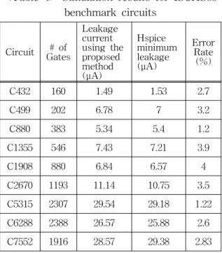
Table 4 shows the summary of the results of the proposed method and Hsice simulation. The first column shows the measured circuits, and the second column is the number of gates of the circuits. The third is the leakage current estimated by our proposed method. The forth shows the Hspice simulation results which are the lowest leakage currents generated by the random simulation(Monte carlo simulation). Finally, the fifth is the error rate between our proposed method and Hspice simulation. The accuracy of the proposed method is within 5% difference compared with Hspice results.
<Table 4> Simulation results for ISCAS85 benchmark circuits
Circuit # of Gates
Leakage current using the proposed method (μA)
Hspice minimum leakage (μA)
Error Rate(%)
C432 160 1.49 1.53 2.7
C499 202 6.78 7 3.2
C880 383 5.34 5.4 1.2
C1355 546 7.43 7.21 3.9
C1908 880 6.84 6.57 4
C2670 1193 11.14 10.75 3.5
C5315 2307 29.54 29.18 1.22
C6288 2388 26.57 25.88 2.6
C7552 1916 28.57 29.38 2.83
6. Conclusion
As technology scales down below 90 nm, the leakage
power becomes a critical issue. This paper proposed a heuristic approach based on a new precise macromodel to generate the input pattern that minimizes the leakage current during standby mode in nanoscale VLSI circuits. The proposed approach uses a new precise macro-modeling of leakage current, considering sub-threshold leakage, gate tunneling leakage, and BTBT leakage component.
The macromodel is developed for every gates in the library that is designed using the 45 nm BSIM4 model of Berkeley Predictive Technology Model (BPTM).
References
[1] N. Verma, ”Analysis Towards Minimization of Total SRAM Energy Over Active and Idle Operating Modes ”, IEEE Tran. on Very Large Scale Integration (VLSI) Systems, Vol. 19, Issue 9, pp. 1695-1703, Sept. 2011.
[2] A. Agarwal, S. Mukhopadhyay, C.H.Kim, et al.,
”Leakage power analysis and reduction: models, estimation and tools”, IEE Proceedings - Computers and Digital Tech- niques, Volume 152, Issue 3, Page(s) 353-368, May 2005.
[3] S. G. Narendra, A. Chandrakasan, ”Leakage in Nanometer CMOS Technologies (Series on Integrated Circuits and sytems)”, Springer, Nov.
2005.
[4] Y. Wang, X. Chen, W. Wang, Y. Cao, Y. Xie, H. Yang, ”Leakage Power and Circuit Aging Cooptimization by Gate Replacement Techniques”, IEEE Tran. on Very Large Scale Integration (VLSI) Systems, Vol. 19, Issue 4, pp.
615-628, April. 2011.
[5] Feng Gao, John P. Hayes, ”Exact and Heuristic
Approaches to Input Vector Control for Leakage
Power Reduction, Computer Aided Design”,
ICCAD-2004, Page(s)527-532, Nov. 2004.
[6] Xiaotao Chang, Dongrui Fan, et al., ”Soc Leakage Power Reduction Algorithm by Input Vector Control”, System-on- Chip,2005, Page(s)86-89, Nov. 2005.
[7] D. Shurin, E. Kvaktun, A. Fish, "Input Vector Control efficiency in sub-micron CMOS technologies," IEEEI 2010, pp. 569-573, Nov.
2010.
김 경 기 (Kyung Ki Kim)