Linearization Method Using Variable Capacitance in Inter-Stage Matching Networks for CMOS Power Amplifier
Jaehyuk Yoon
*, Changkun Park
**★Abstract
In this paper, a watt-level 2.4-GHz RFCMOS linear power amplifier (PA) with pre-distortion method using variable capacitance with respect to input power is demonstrated. The proposed structure is composed of a power detector and a MOS capacitor to improve the linearity of the PA. The pre-distortion based linearizer is embedded in the two-stage PA to compensate for the gain compression in the amplifier stages, it also improves the output P1dB by approximately 1 dB. The simulation results demonstrate a 1-dB gain compression power of 30.81 dBm at 2.4-GHz, and PAE is 29.24 % at the output P1dB point.
Key words :AM distortion, linearity, power amplifier, power detector, pre-distortion, virtual ground
* Agency for Defense Eevelopment
** School of Electronic Engineering, Soongsil University
★ Corresponding author
E-mail:[email protected], Tel:+82-2-828-7166
※ Acknowledgment
This research was supported by Basic Science Research Program through the National Research Foundation of Korea(NRF) funded by the Ministry of Science, ICT & Future Planning(2015-036938).
Manuscript received Jun. 7, 2019; revised Jun. 11, 2019; accepted Jun. 13, 2019.
This is an Open-Access article distributed under the terms of the Creative Commons Attribution Non-Commercial License (http://creativecommons.org/licenses/by-nc/3.0) which permits unrestricted non-commercial use, distribution, and reproduction in any medium, provided the original work is properly cited.
Ⅰ. Introduction
Recently, the CMOS power amplifier (PA) has been widely studied to overcome problems in the feasibility of the PA using a compound semiconductor.
Generally, the limitation of the CMOS PA is linearity. Thus, we must overcome this limitation for a single-chip and achieve size reduction with low cost. Additionally, we require more back-off in a CMOS PA to retain linearity that causes decreasing PAE at the P1dB point. Linearization methods are separated into that feedback, feed- forward, and pre-distortion [1]-[6]. The feedback technique is the most popular because its simple structure allows for easy implementation. It requires only a resistor and a capacitor. However, a problem in stability rises frequently. The feed-forward
method serves as an improved linearization method with high accuracy. However, it has the disadvantage that the required system size to realize the feed-forward method is very bulky compared to the other linearization method. The pre-distortion technique using an analog signal is also one of the most popular linearization methods because of its very simple structure. However, it has high power dissipation and is bulky. In this paper, we propose a linearization technique using the power detection method with a 2nd order harmonic in virtual ground of the drive amplifier. Using the proposed method we can obtain the simple pre- distortion structure and improve gain compression.
To prove the feasibility of the proposed structure, we design the proposed PA as well as a conventional PA with an operating frequency of 2.4-GHz.
105
Fig. 2. Overall architecture.
Fig. 3. Simulated fundamental and second order harmonic
power versus RF input power. Fig. 4. Simulated operation of power detector.
Fig. 1. Concept of proposed PA.
Ⅱ. Proposed Linearization Technique
In this work, we reduce AM distortion using the pre-distortion technique. The gain compression problem arises in high power region of the PA because the non-linear characteristic of the amplifier generate 3rd order harmonic that reduce the power of the fundamental signal. To alleviate the gain compression problem, we design a PA using the pre-distortion technique. Fig. 1 shows conceptual block diagrams of the proposed PA
using the pre-distortion technique.
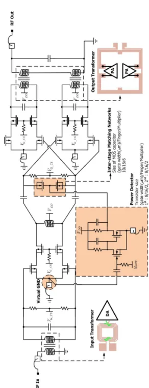
1. Overall Architecture
We designed a differential structure PA using the pre-distortion technique as shown in Fig. 2.
The fundamental and 2nd order harmonics are
proportional to the input and output power which
are shown in Fig. 3. To detect the power of the
signal, we use the 2nd order harmonic at the
virtual ground of the drive amplifier. The detected
AC signal can be converted to a DC voltage by a
power detector. After that, the output power of
the detector is used to control the variable
capacitor and quality factor of the inter-stage
matching network. Finally, the overall 1-dB gain
compression power of the PA was increased to
compensate for the gain compression induced by
the non-linear device. Thus, we can obtain a
wider available power range a result of higher
linearity than a conventional PA.
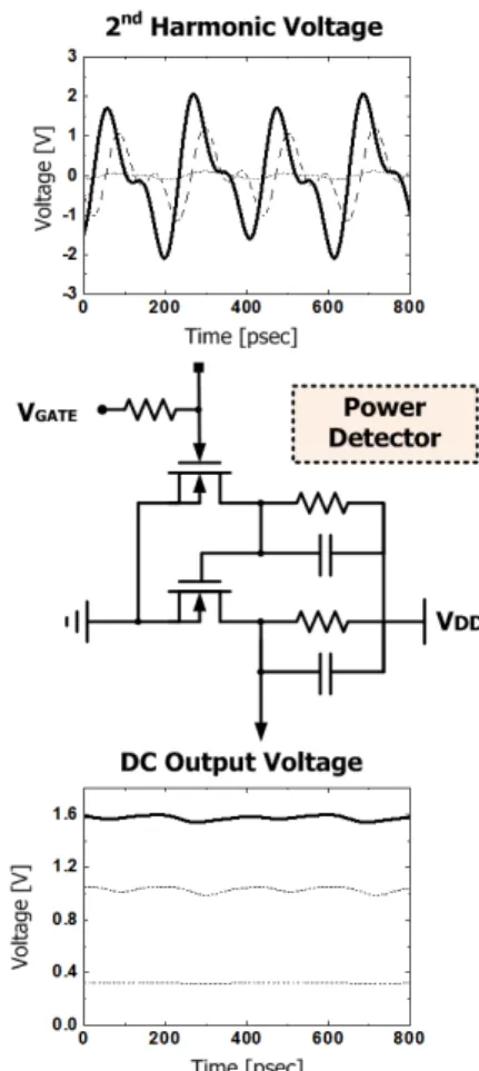
2. Power Detection Method
The power detection scheme is very important for the pre-distortion technique. Generally, we use the input or output signal to detect the signal power [7]. However, this method causes many problems. For example, if we use the input signal of the amplifier for detection, this method reduces the gain of the amplifier and distorts the input signal. Additionally, if we use the output signal of an amplifier, we cannot avoid degradation of the power efficiency. Therefore, we use the 2nd order harmonic to detect the signal power without distortion of the input signal or degradation of the power efficiency. The proposed power detection scheme is shown in Fig. 4. The differential structure must generate the virtual ground induced by the bonder wire at the common ground node of the differential amplifier. To detect the power of a signal, we use the virtual ground in the drive amplifier as an input to the power detector to control the output DC voltage according to the power of the signal. Additionally, we have the ability to adjust the proper bias level to compensate for gain compression. Fig. 5 show the result of operating the power detector according to the gate bias level. Depending on the simulation result, we can determine a proper bias level which is 0.9 V at the 1-dB gain compression point in a conventional PA.
Fig. 5. Simulated power detector output DC voltage versus RF input power.
3. Inter-Stage Matching Networks
We proposed pre-distortion technique using variable capacitor to reduce the problem of gain compression in the high power range. Fig. 6 shows the full-schematic of the proposed PA.
The capacitance is proportional to the quality factor in inter-stage matching networks. It can be described as follows:
Quality Factor = ω
0RC
MOScapacitor(1)
Fig. 6. Full-schematic of the proposed linear PA using
pre-distortion method.
We designed a MOS capacitor that connects the source with the drain of the transistor to operate the variable capacitor. Based on the area, the MOS capacitor has a higher changed value of the capacitance than the PN-varactor, as shown in Fig. 7. The total changed capacitance values are 0.67 pF in the MOS capacitor and 0.35 pF in the PN-varactor from 0.3 V to 1.8 V. The difference in the values is approximately double.
If we use the PN-varactor, which has a lower changed capacitance, we need a larger gate width.
Fig. 7. Simulated capacitance and quality factor of variable capacitors.
The changed value of the quality factor is shown in Fig. 7. We can obtain a higher changed quality factor by using a MOS capacitor instead of a PN-varactor as a variable capacitor. The operation of the variable capacitor in the inter- stage matching network is analyzed with regard to two aspects. First, at the 1-dB gain compression point, the total gain compression point of the PA is enhanced by increasing the quality factor of the inter-stage matching networks induced by the growing parallel capacitance. More specifically, the second harmonic power at the virtual ground of the drive amplifier passes through the power detector. After that, the AC signal is converted to a DC voltage from 0.3 V to 1.8 V. The output of the power detector increases with the capacitance in the inter-stage matching network because of
the difference in the DC voltage between the input bias level of the PA and the output of the power detector. The quality factor of the inter- stage matching network is increased at the 1-dB gain compression point in a conventional PA.
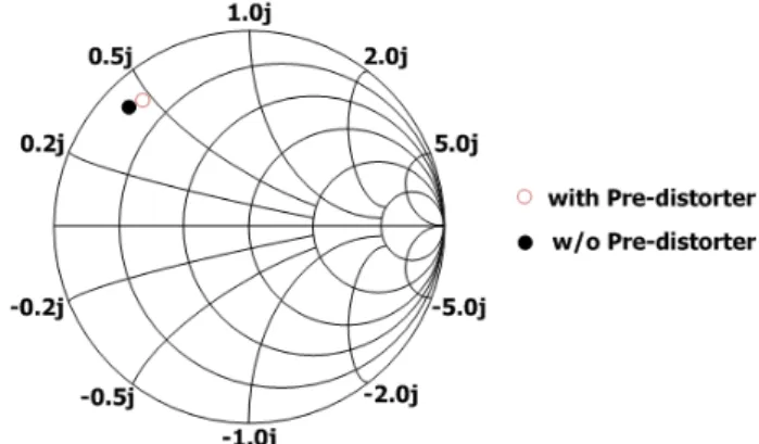
Fig. 8. Simulated Smith-chart of input node at PA.
Additionally, the variable capacitance can change the input impedance of the PA. As shown in Fig.
8, the input impedance of the PA is changed because of the changed capacitance in the inter- stage matching networks. However, the variation in capacitance is smaller than the total capacitance, which is the sum of the parasitic capacitance of the drive amplifier and the parasitic capacitance of the PA. According to the above analysis, we can mitigate the gain reduction problem.
Ⅲ. Design of the CMOS Power Amplifier Using the Proposed Method
In this work, we designed a fully-integrated linear PA using 110-nm RFCMOS technology with eight metal layers. We also designed a conventional amplifier for a fair comparison of the performance levels of the proposed structure.
Both the conventional and proposed PA used a
cascode and differential structure. Additionally,
we used a series power-combining technique to
obtain watt-level output power. To obtain simulation
results closer to the real measurement results,
we simulated a PA, including the inductance of
the bond-wires, which have approximately 0.8
nH of bias padding. Furthermore, the bonding inductance of the input and output pads are set to 0.4 nH to connect the two bond-wires to reduce loss.
1. Driver Stage
A driver stage was designed for the differential cascode structure. The differential structure rejects even-order harmonics with the virtual ground and reduces the gain reduction by the wire-bonding effect between the source of the transistor and the ground. To convert from a single signal to a differential signal, an input transformer is used in the input of the drive amplifier. The cascode structure increases the voltage gain. The driver stage is biased in the shallow class-AB region to provide sufficient gain and power to the power stage. Additionally, we obtain both medium power efficiency and high linearity from the shallow class-AB input bias. The size of the CS transistor is 1.280 mm and the size of the CG transistor is 0.640 mm. The supply voltage, V
DDis 3.3 V, and the gate bias of the CS stage is 0.45 V.
2. Power Stage
Two differential pairs of the power stage are designed using a series power combining technique to enhance the output power. Additionally, to obtain watt-level output power, we need to prevent breakdown of the transistor due to high voltage of the output PA. We use a cascode structure and thick gate transistor to avoid a breakdown problem. The power stage is biased in the deep class-AB region to obtain high power efficiency and medium linearity because the power stage consumes higher DC power than the driver stage. The total gate width of the CS transistor is 2.048 mm and the length is 110-nm.
The total gate width of the CG transistor is 4.096 mm and the length is 350-nm. The V
DDis 3.3 V, and the gate bias of the CS stage is 0.42 V.
3. Inter Stage Matching Network
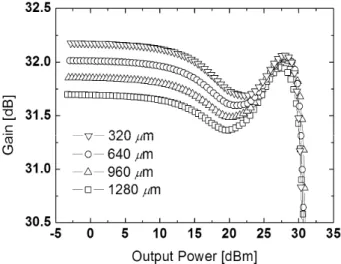
As mentioned above, we use a MOS capacitor to reduce the size of the system. We need to search for the proper gate width for the MOS capacitor. If we use a larger variable capacitor, the problem of gain reduction arises, and the input impedance of the power stage is changed considerably, as shown in Fig. 9. Thus, we select the total width of the variable capacitance which is 0.640 mm to obtain high 1-dB gain compression power.
Fig. 9. Simulated total gate width of MOS capacitor versus output power of PA.
Fig. 10. Simulated gain versus output power of PA.
Fig. 11. Simulated PAE versus output power of PA.
Fig. 12. Simulated DC power consumption of power detector.
Fig. 13. Simulated output power versus input power.
Ⅳ. Results
In this work, we designed a fully-integrated 2.4-GHz linear PA with a differential cascode structure using 110-nm 1P8M RFCMOS technology to verify the feasibility of the proposed technology.
Fig. 10 shows the gain versus the output power of the PAs. As shown in this figure, P1dB of the proposed PA is enhanced by approximately 1 dB compared to the conventional PA because of the pre-distortion effect. Fig. 11 shows the simulated PAE, which reveals that the proposed PA consume more DC power because the power detector consumes very little DC current, from 12.7 mA to 14.7 mA, as shown in Fig. 12.
However, the total DC current consumption of PA is approximately 1.3 A. Therefore, the PAE of the proposed PA is similar to that of the conventional PA with the same output power. As shown in Fig. 13, we can also confirm the power of 3rd-order harmonic, which is similar to that of the conventional PA in the simulation results.
Finally, we summarize the simulation results of the conventional and proposed PAs in Table I.
Table 1. Summary of linear power amplifier performance.
Parameters Conventional PA Proposed PA
PAE@Psat 28.5% @30.7 dBm 30.8% @31.2 dBm PAE@P1dB 25.1% @29.8 dBm 29.2% @30.8 dBmGain 32.3 dB 31.8 dB
VDD 3.3 V 3.3 V
Technology 110-nm 1P8M RFCMOS