900MHz UHF대역 RFID 응용을 위한 Integer-N PLL주파수 합성기 설계
김신웅* · 김영식*
An Integer-N PLL Frequency Synthesizer Design for The 900MHz UHF RFID Application
Sin-woong Kim* · Young-sik Kim*
요 약
본 논문은 전하펌프와 클록트리거 회로를 사용하는 프리스케일러가 포함된 UHF RFID 응용을 위한 900MHz Integer-N 방식의 주파수 합성기를 소개한다. 쿼드러처 출력이 가능한 전압제어발진기와 프리스케일 러, 위상주파수검출기와 전하펌프 및 아날로그 고정 검출기는 0.35-㎛ CMOS 공정으로 설계되었다. 주파수 분 주기는 verilog-HDL 모듈을 통해 설계되었으며 mixed-mode 시뮬레이션을 통해 디자인을 검증하였다. 전압제 어발진기의 동작 주파수영역은 828MHz에서 960MHz이고 위상이 90도 차이나는 쿼드러처 신호를 출력한다.
시뮬레이션 결과로 위상잡음은 100KHz offset 주파수에서 -102dBc/Hz 이었으며, 고착시간은 896MHz에서 928MHz까지 32MHz step을 천이할 때 4us이다.
ABSTRACT
This paper presents an Integer-N phase-locked loop (PLL) frequency synthesizer using a novel prescaler based on a charge pump and clock triggering circuit. A quadrature VCO has been designed for the 900MHz UHF RFID application.
In this circuit, a voltage-controlled oscillator(VCO), a novel Prescaler, phase frequency detector(PFD), charge pump(CP), and analog lock detector(ALD) have been integrated with 0.35-㎛ CMOS process. The integer divider has been developed with a verilog-HDL module, and the PLL mixed mode simulation has been performed with Spectre-Verilog co-simulator.
The sweep range of VCO is designed from 828 to 960 MHz and the VCO generates four phase quadrature signals. The simulation results show that the phase noise of VCO is -102dBc/Hz at 100 KHz offset frequency, and the maximum lock-in time is about 4us with 32MHz step change (from 896 to 928 MHz).
키워드
Integer-N, PLL(Phase-Locked Loop), Quadrature VCO, Prescaler
* 한동대학교 정보통신공학과 접수일자 : 2009. 10. 29 심사완료일자 : 2009. 11. 23
Ⅰ. 서 론 Introduction The frequency synthesizer is a core component in the wireless communication system. It should
provide a clean local oscillation signal to convert an IF signal to RF signal or a RF signal to IF signal.
It’s very important to have a low phase noise level.
Higher phase noise can degrade the system performance by reducing the signal to noise ratio and increasing the adjacent channel interference.
The lower power consumption and high speed operation in a prescaler are very important to reduce the phase in a PLL frequency synthesizer.
This paper proposes a new prescaler circuit having lower power consumption and a high speed operating with lower jitter. Using the prescaler, an integer-N frequency synthesizer has been designed for the UHF band (860-960MHz) RFID.
The UHF band is considered to be suitable to the distribution industry because of a fast data transmission and operation distance [1]. For the lower phase noise level, a LC VCO is designed, and this architecture could relatively get a stable high frequency operation with the current consumption [2]. Recently in the wireless system, according to use a complex modulation method, the LC VCO which is able to generate quadrature waveform is designed. This paper shows the integer-N PLL frequency synthesizer using the quadrature LC VCO (QVCO) and charge pump-based prescaler.
Ⅱ. A Design of Integer-N PLL Frequency Synthesizer
The block diagram of the Integer-N PLL frequency synthesizer is shown in Fig. 1. The VCO, Prescaler, PFD, CP, and loop filter(LPF) have been designed with 0.35-㎛ CMOS process and the integer divider has been implemented with verilog-HDL. The designed VCO is shown in Fig. 2.
This LC quadrature VCO generates 828 to 960 MHz outputs with 4 phases, and the phase difference between adjacent clocks is 90
degree [3].
Figure 1. The block diagram of the Integer–N frequency synthesizer
Figure 2. Coupled LC oscillators with quadrature outputs
Fig. 3 shows the proposed prescaler based on a charge pump. The prescaler operation starts with discharge of capacitor C1. After comparing this discharging waveform with reference voltage, the comparator 1 generates a trigger voltage. The Comparator 2 and RS flip-flop function as a monostable multivibrator [4]. At this time, the output of the D flip-flop charges capacitor C1, C2. Lastly, after the output of the D flip-flop goes high again, the operation returns to the initial state.
The dividing ratio could be adjusted with capacitance of capacitors C1, C2, and it is also possible to tune up the dividing ratio of this prescaler with changing the bias current of I0 or reference voltage of comparator 1. By using this prescaler, especially in high frequency system, the
Figure 3. A circuit of charge pump based Prescaler
power consumption could be reduced because a dividing ratio is getting higher; the current consumption is getting lower.
Fig. 4 and Fig. 5 represent PFD and CP [5]. The doubled p-C2 MOS latch is used as TSPC architecture for the PFD.
Figure 4. A circuit of PFD
Figure 5. A circuit of CP
Figure 6. A circuit of ALD
Fig. 6 shows the analog lock detector [6]. If the PLL is in-lock, small pulses, UP and DOWN, come from the PFD. These pulses are filtered out by a RC network. Then, a Schmitt trigger produces a steady state level. A Low level indicates an in-lock condition and a pulse signal of the OUT indicates an out-of-lock condition.
Ⅲ. Results of Frequency Synthesizer Fig. 7 shows the waveform of VCO quadrature output. The range of output frequency is from 828 to 960MHz and the phase difference is 90 degree each. The phase noise of VCO is -102dBc/Hz at 100 KHz offset frequency and the current consumption is 6.34mA. Fig. 8 shows the waveform of prescaler. Each alphabet means the waveform of each node in Fig. 3.
The dividing ratio is 8 and the current consumption of buffer is 2.8mA and the others are 894.6uA.
Figure 7. A Simulation result of VCO
Figure 8. A Simulation result of Prescaler
Fig. 9 shows the control voltage pattern of VCO and output of the analog lock detector when the PLL is locked. It is measured when the VCO frequency varies from 896 to 928MHz. The bandwidth of LPF is 400 KHz and the lock-in time is about 4us.
Figure 9. A Simulation result of PLL
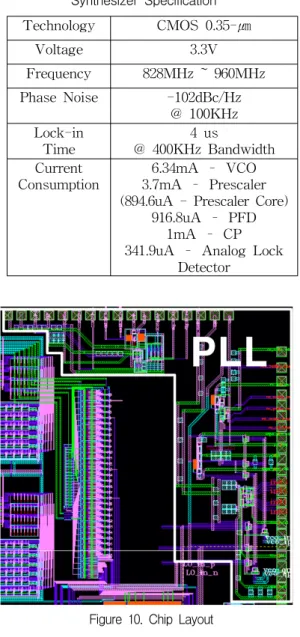
Table I shows the performance results of a designed PLL frequency synthesizer. Fig. 10 represents the photograph of the PLL layout.
TABLE I. The Integer-N PLL Frequency Synthesizer Specification
Technology CMOS 0.35-㎛
Voltage 3.3V
Frequency 828MHz ~ 960MHz
Phase Noise -102dBc/Hz
@ 100KHz Lock-in
Time
4 us
@ 400KHz Bandwidth Current
Consumption
6.34mA – VCO 3.7mA – Prescaler (894.6uA - Prescaler Core)
916.8uA – PFD 1mA – CP 341.9uA – Analog Lock
Detector
Figure 10. Chip Layout
Ⅳ. Conclusion
An Integer-N PLL frequency synthesizer has been designed using a prescaler based on a charge pump and VCO which is able to generate quadrature waveform for 900MHz RFID technology. The VCO, Prescaler, PFD,
and CP are implemented with 0.35-㎛ CMOS Process and integer divider is designed with verilog-HDL. The simulation results show that the phase noise of the quadrature VCO is -102dBc/Hz at 100 KHz offset frequency.
When the bandwidth of LPF is 400 KHz, lock-in time is 4 us. The operating voltage is 3.3V.
Acknowledgement
This research was financially supported by the Ministry of Coomerce, Industry and Energy (MOCIE) and Korea Industrial Technology Foundation (KOTEF) through the Human Resource Training Project for Regional Innovation.
This work was supported by IDEC through the MPW program.
Reference
[1] Cheolsik Pyo, “UHF RFID”, TTA Journal, No.94, pp.123, July 2004.
[2] William F. Egan, “Frequency Synthesis by Phase Lock”, Wiley Inter-science, 1999.
[3] Ibrahim R. Chamas, “Analysis and Design of a CMOS Phase-Tunable Injection-Coupled LC Quadrature VCO (PTIC-QVCO)”, IEEE Journal of Solid State Circuits, Vol.44, No.3, March 2009.
[4] Sedra and Smith, “Microelectronic Circuits, fifth edition”, OXFORD, pp.1200, 2007 [5] R. Jacob Baker, “CMOS-circuit design, layout,
and simulation, 2nd edition”, Wiley Inter- science, pp.551-561, 2008.
[6] Den Dulk and R.C, “Digital PLL lock-detection circuit” IEEE Electronic Letters, Vol.24, No.14, pp.880-882, July 1988.
김영식(Young-sik Kim) 1993년 2월 : 포항공과대학교 전자 전기공학과 (공학사)
1995년 2월 : 포항공과대학교 대학 원 초고주파공학과 (공학석사) 1999년 2월 : 포항공과대학교 대학원 초고주파공학과 (공학박사)
※관심분야 : 센서 네트워크 개발, RFID, 무선 송수 신용 RF/Analog IC설계, 무선통신용 모뎀 설계
저자 소개
김신웅(Sin-woong Kim) 2009년 2월 : 한동대학교 전산 전자 공학부 (공학사)
2009년 2월 : 한동대학교 정보 통신 공학과 석사과정
※관심분야 : RFID/USN, VLSI 설계, 주파수 합성기 설계, RF/Analog IC 설계

![Fig. 4 and Fig. 5 represent PFD and CP [5]. The doubled p-C2 MOS latch is used as TSPC architecture for the PFD](https://thumb-ap.123doks.com/thumbv2/123dokinfo/5420430.426299/3.774.86.696.160.448/fig-fig-represent-pfd-doubled-latch-tspc-architecture.webp)
![Fig. 6 shows the analog lock detector [6]. If the PLL is in-lock, small pulses, UP and DOWN, come from the PFD](https://thumb-ap.123doks.com/thumbv2/123dokinfo/5420430.426299/4.774.414.703.122.376/fig-shows-analog-lock-detector-pll-small-pulses.webp)