A High Performance Harmonic Mixer Using a plastic packaged device
Jae-hyun Kim*․Min-ho Go*․Hyo-dal Park*․Hyun-sik Shin**
본 연구는 인하대학교 학술연구비 지원에 의해 연구되었음.
ABSTRACT
In this paper, a third-order harmonic mixer is designed using frequency multiplier theory for the Ka-band. The gate bias voltage is selected by frequency multiplier theory to maximize the third-order harmonic element ofthe fundamental LO frequency in the proposed mixer. The designed mixer has a gate mixer structure composed of a gate terminal input for the fundamental local signal (fLO), RF signal (fRF) and a drain terminal output for the harmonic frequency (3fLO-fRF) respectively. The Ka-band harmonic mixer is designed and fabricated using a commercial GaAs MESFET device with a plastic package. The proposed mixer will provide a solution for the problems found in the high cost, complex circuitry in a conventional Ka-band mixer. The 33.5 GHz harmonic mixer has a -10 dB conversion gain by pumping 11.5 GHz LO with a +5 dBm level.
Keywords
Harmonic, High Order, Mixer, Plastic Package.
* 인하대학교 전자통신공학과 ** 전남대학교 전자통신공학과 접수일자 : 2007. 01. 17 심사완료일자 : 2007. 02. 25
I. Introduction
Over the last ten years, there has been an unprecedented growth in the number of systems that use the microwave and millimeter wave bands. The design parameters, such as low cost, high per- formance and reproducibility, are important consi- derations to design in microwave and millimeter wave systems[1]. The SHP(Sub-Harmonically Pum- ped) mixer, using an anti-parallel diode, has been used in the microwave and millimeter bands because of the advantage of low LO frequency, low spurious response, and noise suppression. But many sub-h-
armonic mixers, with an anti-parallel diode, were used and bonded to the circuit using silver epoxy[2][3] or were fabricated using a MMIC realiz- ation[4] resulting in higher cost and less repro- ducibility. Compared with conventional mixers, with an anti-parallel diode, SHP mixers using a active device which have similar SHP mixer properties as their diode counterparts have been developed, where two active devices are pumped in anti-phase at half of the LO frequency. The active SHP mixers, with anti-phase LO input[5], have a disadvantage of larger size, higher cost, and less reproducibility in their MMIC and Hybrid realization.
In this paper, a Ka-band harmonic mixer, with a plastic packaged active device, is proposed to over- come these disadvantages of previous reported har- monic mixers. This harmonic mixer designis based on the multiplier theory that
there is a bias point to maximize a specific harmonic order with respect to a fundamental LO frequency. This can get the high-order mixing element (fRF±3fLO) to be greater than other mixing elements, pumping a RF frequency (fRF) and LO frequency (fLO), because of the bias voltage for the maximum third-order harmonic element (3fLO).
The proposed harmonic mixer described in this paper offers several advantages over that of con- ventional SHP(Sub-Harmonically Pumped) mixers or high-order harmonic mixers. Similar to using a comm- ercialGaAs MESFET, it gives economical cost and good efficiency of production. In addition, the pro- posed mixer has an additional advantage of small size because it does not use an additional phase shift circuit. The paper is organized as follows. SectionⅡ covers the design procedure of the harmonic mixer.
The fabrication and performance of the proposed mixer and conclusion are discussed in section Ⅲ and Ⅳ.
Ⅱ. Harmonic mixer design
1. Bias selection based on multiplier operationThe major nonlinearities inthe FET causing harmonic generation are : 1) the gate-source and gate-drain nonlinear capacitors, Cgs and Cgd, which represent the gate-junction depletion layer capa- citance; 2) the drain current Ids’ nonlinearity, which arises when the current is clipped when Vgs swings below pinch-off and/or swing positive to cause the gate diode, represented by Rgs, to conduct; 3) the nonlinearity of the Vgs-Ids’transfer characteristics, which in the present instance is assumed to be quadric, but in practice is more complex ; and 4) the
output conductance nonlinearity. But the drain clip- ping is the most impressive effect on the harmonic generation as compared with to others’ nonlinear elements[6][7].
An even harmonic occurs when the output current or output voltage’s waveform is distorted asym- metrically. On the other hand, an odd harmonic occurs when the output waveform is distortedsy- mmetrically to positive peak. Those effects are con- trolled by bias or drain termination.
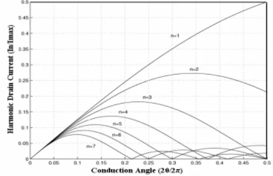
The gate bias and gate input signal are selected to maximize the output level of the desired harmonic element by an approximation relating the harmonic drain current to the FET conduction angle. The harmonic drain current can be represented as a Fourier series expansion as a function of conduction angle and can be written as Equation (1) [8].
max 2
2 π I θ
Idc ≈ (1)
Where INis the drain current for the nthharmonic, Idc is the average of the drain current, Imaxis the maximum drain current, and
2θ
is the conduction angle. From Equation (1), Fig. 1 shows harmonic output current as a function of conduction angle.Fig. 1 Normalized harmonic current as a function of the conduction angle.
Conduction angle should be chosen to give high In
in order to maximize the desired harmonic output power. The optimum conduction angle is appro- ximately
2θ=0.23
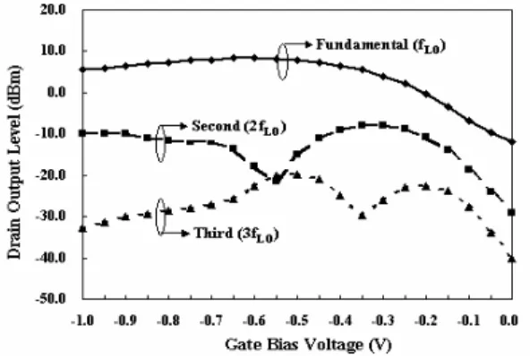
for the maximum third-order harmonic form Fig.1. However, This conduction angle equal to C class-bias conduction is not proper because the input matching is difficult and diode avalanche in the drain-gate is occurred when the gate has high minus voltage. Thus, to generate at the output a signal waveform rich with the desired third harmonic, biasing the device in a A-class and overdriving it until there is a clipping due to pinch-off on the negative swing and due to gate conduction on the positive swing [9].Fig. 2 shows the output power level of a fun- damental (fLO), second harmonic (2fLO) and third harmonic (3fLO) element of a local signal by adjusting gate bias voltage for the applied LO signal. From Fig.
2, there is a specific gate bias voltage where the third harmonic is the maximum.
Fig. 2 Output harmonic generation as function of gate bias voltage.
2. The stability design of the circuit
The feedback of a fundamental element and harmonics at the drain can result in an unstable circuit. The sufficient elimination of unwanted har- monics and the proper stabilization of the circuit, even if some of the conversion gain must be sac- rified, can be adjusted to ensure stability. Fig. 3(a)
showsthe circuit for stable operation with the gate bias in maximizing the third harmonic frequency as in the previous step. The input bias network typically includes a high impedance quarter wavelength line at the fundamental frequency (fLO). This is so that no fundamental power leaks into the DC bias and acts as a short-circuit at the second harmonic frequency (2fLO) as it becomes half wavelength at the second harmonic (2fLO). The open stub at the gate acts as a short-circuit at the third harmonic frequency (3fLO) fed from the drain port. The output circuit also provides sufficiedt rejection of harmonics, and provides short-circuit terminations to harmonics at the drain to ensure stability. The open stub at the drain acts as a short-circuit at the fundamental harmonic frequency (fLO). Fig. 3(b) shows the sta- bility factor of the circuit be greater than one over the full frequency band.
(a)
(b)
Fig. 3 (a) Circuit (b) Stability factor with respect to frequency.
3. The port selection for signal injection to realize a mixer circuit.
Single active mixers are generally categorized into one of three topologies; (1) gate, (2) drain, and (3) source mixers. In the case of the gate mixer, both LO and RF signals are applied to the gate while the IF is extracted from the drain terminal. The FET is biased near pinch-off so that the applied LO signal can modulate the transconductance of the FET over a highly nonlinear operating regime. For the drain mixer, the LO and RF signals are applied to the drain and gate, respectively, while the IF signal is extracted from the drain. This mixer operates with the FET drain-source voltage near the knee region.
In a source FET mixer, the LO and RF signals are fed into source and gate respectively while the IF signal is extracted from the drain. This topology allows a modest degree of LO-to-RF isolation. Since the source FET mixer does not require a coupler or combiner, it is a simple structure compared with ot- her mixer topologies. However, this configuration requires careful bypassing technique in the source for the IF frequency in order to suppress instability.
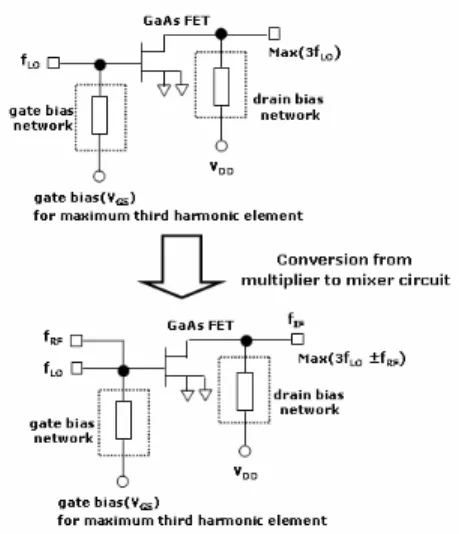
Fig. 4 The concept of converting from multiplier to mixer circuit.
Fig. 4(a) shows the conversion from the designed circuit based on multiplier theory to mixer circuit.
The gate bias voltage is selected to maximize the third harmonic signal (3fLO) by the previous section.
The local frequency (fLO) and the radio frequency (fRF) are inputted to the gate and the intermediate frequency (fIF) is outputted to the drain as a gate mixer structure, which has higher conversion gain then other mixer topologies such as drain mixer and source mixer[10].
Fig. 5 shows the structure of the proposed har- monic mixer, The local frequency (fLO) and radio frequency (fRF) to input gate after each matching, and IF signal (fIF) is to the drain after the low pass filter.
The gate bias voltage of the proposed mixer is selected on multiplier theory to maximize the third harmonic signal (3fLO). The LO matching circuit is designed by a large signal scattering parameter as a large signal LO is applied. The matching circuit of the RF and IF ports is designed as quasi-linear be- cause the RF and IF ports of impedance are affected by LO signal level[11].
Fig. 5 The proposed harmonic mixer configuration.
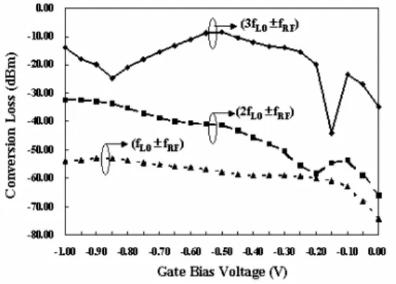
The gate bias voltage of the proposed harmonic mixer is selected to make the mixing component between the applied RF signal (fRF=33.5 GHz) and third harmonic signal (3fLO=34.5 GHz) of the pumped fundamental LO signal (fLO=11.5 GHz) to be maxi-
mum, which let the conversion loss be minimum at the immediate frequency (fIF=3fLO-fRF=1.0 GHz).
Fig. 6 shows the conversion loss characteristic of the harmonic mixer as a function of gate bias voltage. Fig. 6 delineates the frequency conversion characteristic (3fLO-fRF) generated by the third-order harmonic component (3fLO). As seen from Fig. 6, the conversion loss is -10dB when the gate bias voltage (Vgs) is -0.5V for maximum third harmonic ge- neration and also shows conversion loss characte- ristics for both the harmonic mixing component (fLO-fRF) by the fundamental LO signal and the harmonic mixing component (2fLO-fRF) by the second LO signal.
Fig. 6 The conversion loss of the third-order harmonic mixing and fundamental , second harmonic mixing.
Ⅲ. Measurement Result
The proposed mixer fabrication is fabricated on a Teflon substrate, which has dielectric constant 2.17, 0.5mm substrate height and 18um conductor thic- kness.
Fig. 7 shows the measurement results of conversion loss performance at the immediate fre- quency (3fLO-fRF) as a function of gate bias voltage when the fundamental LO signal is +5 dBm. Conv- ersion loss is approximately -10dB when the gate voltage is -0.5V. As seen from the result, the con-
version loss is rapidly decreased at other bias points except the gate bias voltage, which makes the third harmonic component (3fLO) a maximum.
Fig. 7 The variation of the conversion loss with respect to gate bias voltage.
Fig. 8 shows the conversion loss as a function of the LO level when the gate bias voltage is -0.5V.
The conversion loss is about -10dB when LO level is from +5 dBm to +10 dBm.
Fig. 8 The conversion loss performance with respect to LO power.
The output spectrum is approximately -52.5 dBm when the gate bias voltage is -0.5V with the fun- damental LO level +5 dBm and RF level –40 dBm, as seen in the Fig. 9.
3fLO-fRF
-fLO=11.5 GHz/+5dBm -fRF=33.5 GHz/-40 dBm 3fLO-fRF
-fLO=11.5 GHz/+5dBm -fRF=33.5 GHz/-40 dBm
Fig. 9 IF output spectrum of the harmonic mixer.
Fig. 10 shows conversion loss performance as a function of RF frequency. The conversion loss is -8
~ -10 dB when operating from 33.0 GHz to 36.0 GHz, which is lower than other published harmonic mixers at the Ka-band.
-12.00
-10.00 -8.00
-6.00 -4.00 -2.00
0.00
33.00 33.50 34.00 34.50 35.00 35.50 36.00
Conversion loss(dB)
RF frequency (GHz) -12.00
-10.00 -8.00
-6.00 -4.00 -2.00
0.00
33.00 33.50 34.00 34.50 35.00 35.50 36.00
Conversion loss(dB)
RF frequency (GHz)
Fig. 10 The conversion loss with respect to RF frequency.
Fig. 11 shows the linearity performance of the proposed harmonic mixer when changing the RF signal level (33.5 GHz). As seen from Fig. 12, the 1-dB gain compression point is approximately 0 dBm.
-20.0 -18.0 -16.0 -14.0 -12.0 -10.0 -8.0 -6.0 -4.0 -2.0 0.0
-40.0 -35.0 -30.0 -25.0 -20.0 -15.0 -10.0 -5.0 0.0 5.0 10.0 RF Power (dBm)
Conversion Loss (dB)
Fig. 11 Linearity performance.
Fig. 12 shows the isolation performance at the each port with the same environment for measuring the output spectrum. It is shown that the LO-RF isolation performance, worse than the RF-IF iso- lation, and the LO-IF isolation performance as known a single gate mixer’ disadvantage. Table.1 sum- marizes the performance of the proposed third har- monic mixer.
-70 -60 -50 -40 -30 -20 -10 0
10 12 14 16 18 20 22 24 26 28 30 32 34 36 38 40 주파수[GHz]
RF-IF LO-IF LO-RF
Isolation [dB]
RF frequency [GHz]
RF-IF Isolation
LO-IF Isolation LO-RF Isolation
-70 -60 -50 -40 -30 -20 -10 0
10 12 14 16 18 20 22 24 26 28 30 32 34 36 38 40 주파수[GHz]
RF-IF LO-IF LO-RF
Isolation [dB]
RF frequency [GHz]
RF-IF Isolation
LO-IF Isolation LO-RF Isolation
Fig. 12 Isolation performance.
Table 1. Summary of the proposed harmonic mixer.
Items Design Measurement
Frequency
RF 33.5 GHz
LO 11.5 GHz
IF 1.0 GHz
Lo Power 0 dBm 5 dBm
Conversion loss
@ 33.5 GHz -10 dB -10 dB 1-dB gain compression
point(P1dB) 5 dBm 0 dBm
Isolation
LO-RF - -10 dBm
LO-IF - -58 dBm
RF-IF - -43 dBm
Ⅳ. Conclusion
In this paper, a new design method based on a frequencymultiplier is applied for a harmonic mixer.
The proposed harmonic mixer that has -10dB conversion loss at the immediate frequency (fIF=3fLO
-fRF) by selecting the gate bias voltage which let the third harmonic component (3fLO) of the fundamental LO signal (fLO) to be maximum is designed and fabricated.
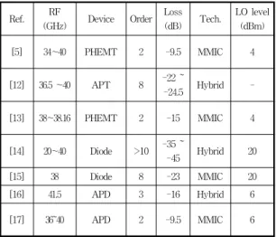
Table 2. Performance comparisons with the other papers.
Ref. RF
(GHz) Device Order Loss
(dB) Tech. LO level (dBm)
[5] 34~40 PHEMT 2 -9.5 MMIC 4
[12] 36.5 ~40 APT 8 -22 ~
-24.5 Hybrid -
[13] 38~38.16 PHEMT 2 -15 MMIC 4
[14] 20~40 Diode >10 -35 ~
-45 Hybrid 20
[15] 38 Diode 8 -23 MMIC 20
[16] 41.5 APD 3 -16 Hybrid 6
[17] 36~40 APD 2 -9.5 MMIC 6
Table.2 presents performance comparisons with other referenced papers. As compared with the other papers, the proposed harmonic mixer has many advantages, not only in electrical performance such as low conversion loss, but also in cost and circuit complexity by using a commercial GaAs MESFET with a plastic package.
ACKNOWLEDGEMENT
This work was supported by the Incheon IT Promotion Agency for "The Development work of technical service and complex terminal test with embeded base on RFID for air cargo".
REPERENCE
[1] A R Barnes, P Munday, R Jennings and M T Moore, "A comparison of W-band mon- olithic resistive mixer architectures", IEEE MTT-S Digest, pp.1867-1870, 2002.
[2] Tsz Yin Yum, Quan Xue and Chi Hou Chan, "Novel sub-Harmonically Pumped Mixer Incorporating Dual-Band Quarter-Wave and In-Line Stub", IEEE MTT-S Digest, pp.87-90, 2003.
[3] Ji-Young Park, Seong-Sik Jeon, Yuanxum Wang and Tatsuo Itoh, "Millimeter wave Direct Quadrature Integrated with Antenna for Broad-band Wireless Communications", IEEE MTT-S Digest, pp1277-1280, 2002.
[4] P. Bernkopf and Y. Tajima, "A Monolithic Ka-Band Sub-Harmonically Pumped Freq- uency Converter", IEEE Microwave and millimeter-Wave Monolithic Circuits Symp- osium, pp.43-46, 1991.
[5] K. S. Ang, A. H. Baree, S. Nam and I. D.
Robertson, "A Millimeter-Wave Monolithic Sub-Harmonically Pumped Resistive Mixer
", in 1999 Int. Microwave Symp. Dig., pp.222-225.
[6] Anand Gopinath, "Single-gate MESFET FET frequency dublers", IEEE Trans Microwave Theory Tech. Vol. MTT-30, No. 6, pp.869-874, June 1982.
[7] C. Rauscher, "High-frequency doubler ope- ration of GaAs field effect transistors", IEEE Tans. Microwave Theory Tech. Vol.
MTT-31, No. 6, pp.462-473, June 1983.
[8] E. O’ciardha, "Generic-device frequency multiplier analysis a unified approach", IEEE Trans. Microwave Theory Tech., Vol.
MTT-48, No. 7, pp.1134-1141, July 2000.
[9] H. Fudem and E. C. Niehenke, "Novel mil- limeter wave active MMIC triplers", IEEE MTT-S Int. Microwave Symp. Digest, pp.
387-390, May 1998.
[10] M. Fairburn, B. J. Minnis, J. Neale, "A novel monolithic distributed mixer design", IEEE Colloquium on Microwave and Millimeter Wave Monolithic Integrated Circuits, pp.13/1-13/6, Nov. 1988.
[11] Yew Hui Liew and Jurianto Joe, "RF and IF ports Matching Circuit synthesis for a Simultaneous Conjugate-Matched Mixer Us- ing Qualsi-Linear Analysis", IEEE Trans.
Microwave Theory and Tech, Vol.50, No.7, pp.2056-2062, Sep. 2002.
[12] Yang Tao, Yand Xiao Bo and Liu Ren Hou,
"Ka-Band Preselected Harmonic Mixer", IEEE, pp.455-456, 2000.
[13] Yon-Lin Kok, Morteza Ahma, Huei Wang, Barry R. Allen and Tzuen Lin, "A Ka-Band Monolithic Single-Chip Transceiver Using Sub-harmonic Mixer", IEEE MTT-S Digest, pp.309-311, 1998.
[14] Tiberiu Mazilu and Ashok K. Talwar, "Har- monic Mixer for the 20-40 GHz Range", IEEE Trans. Microwave Theory and Tech., Vol.MTT-30, No.1 pp.106-107, Jan. 1982.
[15] Weiwei Zhao, Claus schollhorn, Erich Kasper and Clemens Rheinfelder, "38GHz Coplanar Harmonic Mixer on Silicon", pp.
138-147, 2001.
[16] Pascual M.L and Hartnage H.L, "An Optimal Mixer Matching Design Technique Under Large Signal Pumping", rfdesign Journal, pp.28-38, Jan. 2003.
[17] Kenji Itoh, Akio Iida, Yoshinobu Sasaki, Shuji and Shuji Urasaki, "A 40 GHz Band Monolithic Even Harmonic Mixer with An Antiparallel Diode Pair", IEEE MTT-S Di- gest, pp.879-882, 1991.
AUTHORS
Jae-hyun Kim
received the B.S.E.E. degree in ele- ctronic engineering from University of Incheon , Incheon, Korea, in 2003. and he is currently working toward the M.S. degree at the INHA University at Inc- heon, where his work is focused on Microwave system, Power amplifier, MMICMin-ho Go
received the B.S.E.E. degree in electronic communication engineering from Yosu National University, Jeo- nnam, Korea, in 1995, the M.S.E.E.
degree in electronic engineering from the INHA Uni- versity, Incheon, Korea, in 1997. and he is currently working toward the Ph.D. degree at the INHA University.
where his work is focused on Wireless communication system, Microwave system, Antenna, RFIC.
Hyo-dal Park
received the B.S.E.E degree in electronic engineering from INHA University, Incheon, Korea, in 1978, and the M.S. and Ph.D. degrees from the ENSEA, France, in 1984 and 1987. He is currently a Professor with the School of electronic engineering from the INHA University, Incheon, Korea.
For five yesrs, he was a researcher with Center National Recherche Scientifique(CNRS) and Center National d’Etudes Spatiales(CNES), France, 1983–1987.
His current research concerns Microwave system and Aeronautical Electronics Communication System.
신현식(Hyun-sik Shin)
1969년 2월 광운대학교 무선통신 공학과 졸업(공학사)1980년 8월 건국대학교 행정대학 원(통신행정전공)졸업(행정학 석사) 1995년 8월 경남대학교 대학원(통신정책 전공) 졸업 (행정학 박사)
1978년 4월 여수대학교 전자통신공학과 교수 2006년 3월 전남대학교 전자통신공학과 교수 1997년 7월 한국해양정보통신학회 부회장 2000년 3월 인천국제공항 TRS 기술평가위원 2000년 3월 교육인적자원부장관 위촉 여수대학교 국 정도서편탄위원장
2001년 1월 한국해양정보통신학회장, 현 명예회장 2002년 10월 한국대학교육협의회 대학종합 평가위원 2003년 3월 한국과학기술총연합회 대의원
2003년 5월 제13회 과학기술 우수 논문상 수상 2004년 7월 여수대학교 산업대학원장
2005년 7월 교육인적자원부 교육과정 심의위원 2005년 10월 여수대학교 교육대학원장 2006년 3월 전남대학교 산학협력대학원장