pISSN 1229-3008 eISSN 2287-6251
Progress in Superconductivity and Cryogenics
Vol.16, No.2, (2014), pp.1~6 http://dx.doi.org/10.9714/psac.2014.16.2.001
```
1. INTRODUCTION
Since the discovery of a high temperature superconductor [1-3], lots of effort has been made to realize the HTS applications [4-15]. Among the applications, those using the HTS tape are expected as the promising ones, since the tapes could give a flexible shape for variable performances corresponding to the applications.
There has been two different kinds of HTS tapes, which are BSCCO silver sheathed tapes and Y(RE)BCO coated conductors(CCs). Although the development of the BSCCO tapes was preceded [11, 12], a large-scaled development of CCs was started in FY1999 as the national project in Japan with expectation of the high potential of REBCO material [5, 8, 10]. Through the development of CCs of ten years, a length (L) and a critical current (Ic) had been drastically improved and the reasonable long tapes with high performance typically such as 200m-200 A/cm-width could be prepared [5, 9, 10]. This led to the start of a new national project of the M-PACC project [4, 6].
In this project, verifications of electric power application devices such as a transmission cable, a transformer and a superconducting magnetic energy storage (SMES) system using CCs were carried out as the sub-projects. In parallel, the further development of CCs was also included as another sub-project.
In this paper, the brief summary of the electric power
device verifications and the detailed achievements on the R&D of CCs in the M-PACC project were reviewed.
2. BRIEF SUMMARY OF ELECTRIC POWER DEVICES
The objectives of the M-PACC project are to develop next-generation superconducting electric power devices with CCs and to establish important component technologies to realize a more stable and highly efficient electric power supply system as a part of the economic infrastructure of our society.
2.1. Superconducting Transmission Cable [4, 16, 17]
The cables to be developed in the M-PACC project are relatively shorter in length (e.g. 15, 30 m than those in other projects; however, their development was very challenging in terms of the cable specifications such as high applied voltage and large current capacity. The two different cables with different specifications had been developed as a three-core (3-IN-ONE®, Triad) 66 kV/5 kA large-current cable system and a single-core 275 kV/3 kA high-voltage cable system.
Regarding the development of large-current and low-AC-loss cables, a three-phase model cable was designed and fabricated, with a core consisting of four layers of superconducting CCs for the conductor and two
Progress in R&D of coated conductor in M-PACC project
T. Izumi*, a, A. Ibia, K. Nakaokaa, T. Tanedaa, T. Yoshidaa, Y. Takagia, T. Nakamuraa, b, T. Machia, K. Katayamaa, N. Sakaia, M. Yoshizumia, T. Koizumib, K. Kimurab, T. Katoc, T. Kissd, and Y. Shioharaa
a Superconductivity Research Laboratory, International Superconductivity Technology, Kanagawa, Japan
b SWCC Showa Cable Systems Co., Ltd., Kanagawa, Japan
c Japan Fine Ceramics Center, Aichi, Japan
d Kyushu University, Fukuoka, Japan
(Received 9 June 2014; revised or reviewed 23 June 2014; accepted 24 June 2014)
Abstract
The five-year national project in Japan for R&D of coated conductors and applications, named as the Materials and Power Applications of Coated Conductors (M-PACC) project, was finished at the end of FY2013. The project consists of four sub-themes as cable, transformer, SMES and coated conductors. In the theme of coated conductors, the fabrication process had been developed to satisfy the requirements from the applications such as in-field Ic performance, low AC loss in the long tapes etc. Through the project, the remarkable progress was achieved as follows; a high in-field minimum Ic value over 54A/cm-width under 3T at 77K was realized in a 200m long EuBCO tape with artificial pinning centers of BaHfO3 by the pulsed laser deposition (PLD) technique on the IBAD template. On the other hand, the AC loss reduction was confirmed in the tapes fabricated by both PLD and the metal organic deposition (MOD) techniques by scribing 100m tapes into 10-filamments. Additionally, the mechanism of the delamination phenomenon was systematically investigated and the strength was improved by eliminating the origins of the weak points in the films. Through the development, all targeted goals were accomplished and the several results were appreciated as a world champion data.
Keywords: YBCO, REBCO, coated conductor, Ic, in-field Ic, AC loss, mechanical strength, Je, cost, delamination, APC
* Corresponding author: [email protected]
Progress in R&D of coated conductor in M-PACC project
layers for the shield. The total AC losses of the conductor and the shield at 71 K were 0.4 W/m/phase at 5 kA was confirmed in the cable using 2 mm wide tapes.
For high-voltage and low-dielectric-loss cables, the technologies for insulating to high voltage, joint and reduction of losses were developed. As a typical result, the AC loss of a single-core model cable made of 3 mm wide tapes were reduced to 0.2 W/m/phase for conducting layer with shielding one. On the other hand, the dielectric loss was as low as 0.6 W/m with the use of polypropylene- laminated paper, PPLP®-C as the insulation material of the choice.
2.2. Transformer [4, 18]
In this project, the several important technologies aiming at a 20 MVA were investigated and a 2MVA transformer using CCs were designed, fabricated, and verified as a demonstration device.
A 400 kVA model transformer with a function of fault current limiting was constructed and tested. The results showed no degradation of the model transformer, including its coils, CCs, and joints, after the short-circuit test, with applied overcurrents being 6 times larger than the rated currents of 174 A at 66 K.
In order to demonstrate the low AC loss in a coil form, a model coil with a scribed conductor was fabricated and tested. The coil was made of a single piece of a scribed five-filament conductor, with the length of 70 m. It was wound 10 times for each layer, and 19 layers to make up a coil. The AC loss of the model coil so constructed was one-fifth of that in the case with a CC without scribing.
A 66kV/6.9kV 2MVA class superconducting transformer was designed including a high-efficiency and compact reverse Brayton cycle refrigerator. On the basis of the design, such a system was constructed and the expected performance was confirmed.
2.3. SMES [4]
A 2 GJ class large-capacity SMES system to be developed in the M-PACC Project was expected to meet the requirements for stable and compact electric power grid control system technology. The main issues in the 2 GJ class SMES system are the development of large-current-capacity conductors made of YBCO CCs and the realization of compact coils wound using large-capacity conductors.
They manufactured component coils (outer diameter 650 mm), adopting a bundled conductor that would enable the realization of high strength and low loss, proving that the coils' current capacity was sufficiently large, exceeding 2.6 kA, through a basic verification test for energization. In addition, the unique coil construction, “Yoroi-coil”, was developed and it could realize high proof abilities against both the thermal stresses and the electromagnetic hoop stress.
3. THEMES & GOALS OF CCs DEVELOPMENT Among the specifications required for the future
Table 1
THEMES AND THE GOALS IN CCS DEVELOPMENT.
Themes Goals
Degradation of
Properties Evaluation of degradation by Humidity etc.
Delamination behavior and its counter-plan High Ic under
Magnetic Fields 50A/cm-w @77K, 3T – 200m 400A/cm-w@65K, 0.1T-100m Low AC Loss 2mm-w – 500A/cm-w @77K,s.f.-200m
5mm-w – 10filaments
Loss Reduction to 1/10 High Strength
& High Je
500A/cm-w – 1GPa @77K,s.f. -50m Je=50kA/cm2 – 200m
Low Cost
& High Yield Low cost toward $20/kAm
Fig. 1. Ic degradation due to humid atmosphere at difference temperature.
applications such as cable, transformer and SMES on the marketable stage, the similar issues are overlapped such as high in-field performance, low AC loss etc. Then, the issues to be developed were classified into 5 categories and those were set as the themes in this sub-project of CCs development. The targeted goals in this sub-project were determined based on the requirements from the future applications as shown in Table 1 [6].
4. ACHIEVEMENTS IN DEVELOPMENT OF CCs 4.1. Degradation of Properties
The degradation due to lots of reasons such as humidity, bending, thermal hysteresis etc. has been quantitatively evaluated. For example, the Ic degradation due to exposure to a high humidity atmosphere was evaluated by investigating the time (R) when the Ic value deteriorates to 95% of an initial one at several different temperatures in order to estimate the limiting period in the worst storage condition such as 313 K (40 C) and RH100%. Figure 1 shows the 1/T dependence of R. According to the extrapolating of the experimental results, the limiting period was estimated to be about 9 years.
Additionally, a delamination behaviour is also investigated [6, 19]. The delaminated interfaces were detected by observation of the starting point of the delamination for many samples which were fabricated by the different processes and/or growth conditions. Through 2
T. Izumi, A. Ibi, K. Nakaoka, T. Taneda, T. Yoshida, Y. Takagi, T. Nakamura, T. Machi, K. Katayama, N. Sakai, M. Yoshizumi, T. Koizumi, K. Kimura, T. Kato, T. Kiss, and Y. Shiohara
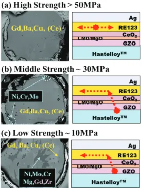
the investigation as shown in Fig.2, it was found that the correlation between the delamination strength and the delaminated interface was classified into three groups. In the group of low strength range around 10 MPa, all samples have the bed layer of Gd-Zr-O fabricated by an MOD process and the layer appeared in the delaminated interface.
Then, the starting point was estimated in the MOD bed layer. On the other hand, the starting point of middle strength range around 30 MPa was considered to occur at the interface between a metal substrate and the bed layer. If the origins of the above mentioned starting points can be eliminated, the tapes should reveal a high delamination strength over 50 MPa, with a starting point in the REBCO layer. Based on this idea, the influences of the process conditions had been investigated and found. Then, it was found that the increment of the temperature of the heat treatment for the MOD bed layer and reduction of the deposition time for the PLD process could make the delamination strength higher. Finally, the tapes without low and middle strengths were successfully fabricated.
4.2. High Ic under Magnetic Fields
As a requirement for magnetic applications such as SMES etc., the superconducting performance under magnetic fields should be improved. In this theme, the in-field Ic had been improved by the introduction of artificial pinning center (APC) and/or thickening the superconducting film layers.
In the early stage of the development in the PLD process for superconducting layers, the BaZrO3 (BZO) nano-rods [19, 20] were successfully dispersed and the Jc and/or Ic
performance under the magnetic field, especially for the magnetic field parallel to the c-axis of the GdBCO crystals
Fig. 2. Observation of delaminated interfaces and the estimated starting points of delamination.
in the films, has been improved. However, the in-field Ic
values in thick films was saturated in the thickness dependence of Ic(B). For this problem, BaHfO3 was found to be effective for maintaining the liner relationship between in-field Ic and the GdBCO layer thickness up to 3μm [4, 21, 22]. Then, a high Ic value of 85 A/cm-width at 77 K and 3 T was realized in the BHO doped GdBCO film as shown in Fig.3. According to the TEM observation, nano-rods of BHO are shorter comparing with BZO and inclined from the c-axis of GdBCO films. Additionally, the morphologies of the BHO nano-rods were uniform from the bottom near the CeO2 layer to the surface. Reflecting these features, the BHO doped GdBCO films reveal the isotropic behavior in Jc-B-θ properties and the difference in the shape could not be recognized for the different thicknesses.
Additionally, another advantage of this system was also found. Although the advantages in Jc-B properties to non-doped films at high temperature disappear at low temperature region in the case of BZO doped GdBCO films, those in the BHO doped films is maintained in wider range of temperatures and magnetic field.
Then, it was found that higher Jc properties with maintaining a linier relationship in the thickness dependence could be obtained in the combination of the EuBCO superconducting matrix with BHO as APC. In the case of the EuBCO-BHO system, it was found that the fraction of the current disturbing particles, such as a-axis oriented grains, CuO etc., in the film was reduced comparing with GdBCO-BHO one. Finally, an extremely high in-field Ic value of 141 A/cm-width at 77 K and 3 T was confirmed(Fig.3). This sample was evaluated in a wide range of temperatures and magnetic fields. A 200 m long tape with BHO doped EuBCO is successfully fabricated and a high in-field Ic value of 54 A/cm-width at 77 K and 3 T was recognized as a minimum value. Most recently, a higher minimum Ic value of 108 A/cm-width at 77 K and 3 T was obtained in a 94 m long tape.
Fig. 3. Thickness dependence of Ic-min. at 77 K under 3 T for different RE in the superconducting layer and APC materials.
3
Progress in R&D of coated conductor in M-PACC project
Fig. 4. Zr-element mapping image in the cross sectional image of the films observed by TEM with(a) and without(b) interim annealing.
On the other hand, the BZO nano-particles were disperse in the YGdBCO films derived from the TFA-MOD process [4, 23, 24]. And the heating profile was modified to make the particles finer and more uniform. Through the investigation of the influences of the heating pattern in the crystallization process, it was found that the additional annealing step around 500C in the heating profile is effective for fine and uniform dispersion of BZO nano-particles. This process is called as the interim annealing. Additionally, the coating process was modified to make a uniform thickness of the coating films in the transverse direction. This can prevent crack formation from the edge in the thick films. These developed technologies were applied to fabricate thick films with BZO fine particles. As a result, the high Ic value of 55 A/cm-width at 77 K and 3 T was obtained in a short tape as shown in Fig.4.
Furthermore, the long tape fabrication is also realized and a 200 m long tape with 50 A/cm-width at 77 K and 3 T was realized.
4.3. Low AC Loss
In the case of AC applications, the reduction of AC losses is one of the important factors. Even when the magnetic field is changed, e.g. ramping step even in the DC magnet, a similar hysteresis loss could be a problem to be solved due to its heat generation. In this theme, the technologies to reduce the losses had been developed corresponding to each application.
For a transmission cable, the magnetic field due to the current flow should generate along the surface of the cable.
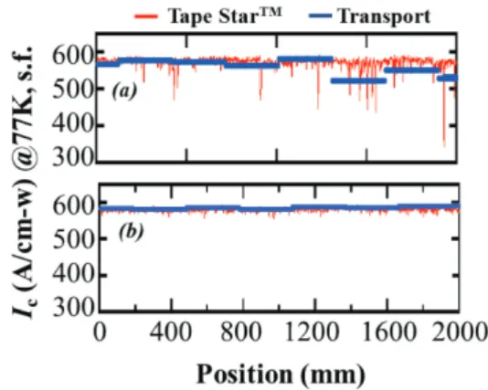
Therefore, if the cable is made with a perfect round shape, the hysteresis loss should not be a problem due to an extremely thin superconducting layer. However, when tape-shaped conductors are used, the edge of the tapes has to be off the circle. Therefore, narrowing the tape width is effective to fit the core for making a circular shape. In this theme, we had made efforts to fabricate CCs with high uniformity and developed cutting technologies with low damage. For these targets, it was found that cleaning process of the buffer layer is effective to remove particle defects. It results in the improvement of the performance uniformity as shown in Fig.5. On the other hand, a cutting technology using a YAG-laser was developed and the condition was optimized for minimizing the damage of the tape. Finally, a high Ic performance was realized in a 200 m long with 2 mm wide tape, which satisfied the targeted goal.
In order to reduce the loss for transformer, in which the transverse magnetic fields to the tapes, it is known that the
Fig. 5. Ic distributions of the long tapes without (a) and with (b) cleaning of CeO2 buffer layer.
narrowing the width of the tapes such as filamentation is effective. Then, the two dimensional uniformity of the Ic
performance is also necessary. And a scribing technique without any serious damages to the superconducting films are required to realize both high performance and low loss properties On the development of the scribing technique, the chemical etching process was optimized to minimize the over-etching region into the REBCO films. As a result, a 100 m long tape with 5 mm in width was divided into 10 filaments and the AC loss reduction of 1/10 was confirmed.
This satisfied the targeted goal of the AC loss reduction [4].
4.4. High Strength & High Je
A large electro-magnetic hoop stress could occur in the high magnetic field applications such as a SMES and a mechanical stress could be loaded for production and installation of application devices such as a drawing process in the transmission cable. In this theme, the strengthening technologies of the metal substrate had been developed and the process conditions for them had been adjusted.
The mechanical strength was improved by modification of deformation process of the HastelloyTM substrate. As a result, the tensile strength of 1GPa was confirmed by the tapes cut from a 200m long tape with a high Ic value over 500 A/cm-width. This result met the targeted goal shown in Table 1.
Additionally, a high engineering current density is necessary to realize compact devices. Especially for an underground cable, a high Je tapes are strongly required since the space of the duct for installation of the cable is limited. A thin metal substrate of 70μm in thickness was prepared. The buffer and superconducting layers were deposited on a 217 m (70 μmt) metal tape with low tension and a high Ic value over 539 A/cm-width at 77K, self-fields was confirmed. It corresponds to the Je value of 52 kA/cm2, which is also higher than the targeted goal.
4.5. Low Cost & High Yield
For all applications, a cost reduction is the one of the important issues as a judgment index for practical usage and industrialization Concerning the development of the lowering technical cost (Yen/Am), the improvement of a 4
T. Izumi, A. Ibi, K. Nakaoka, T. Taneda, T. Yoshida, Y. Takagi, T. Nakamura, T. Machi, K. Katayama, N. Sakai, M. Yoshizumi, T. Koizumi, K. Kimura, T. Kato, T. Kiss, and Y. Shiohara
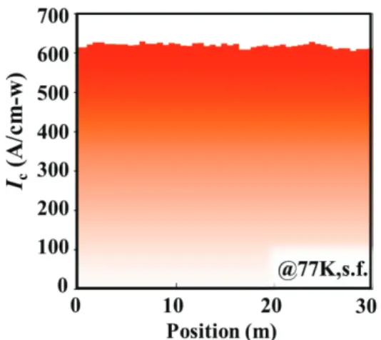
Fig. 6. Ic distribution of the tape which satisfied targeted goal of the project on the cost.
production rate and Ic property is important. In the PLD process, it was found that the higher laser energy density and the high pressure are effective to obtain higher production rates. On the other hand, the interim annealing, which is effective to make BZO particles finer, is also valid to improve Jc property even in the self-field. Then, the low technical cost of 1.6 Yen/Am was achieved both in the PLD and MOD CCs. As an example, Figure 6 shows one of the results obtained in the CC by the TFA-MOD process. In this case, the CC was fabricated at 10m/h for the crystallization step and reveals the higher Ic values than 605 A/cm-width.
5. ACHIEVEMENT TO GOALS
Finally, all targeted goals of the themes in this project, which is indicated in Table 1, were successfully achieved as shown in Table 2.
Table 2
TYPICAL RESULTS ACHIEVED IN M-PACCPROJECT.
Themes Goals
Degradation Properties of
Limiting period in the worst storage condition
= about 9 years
Clarification of the delamination mechanism
Elimination of origins for delamination
>50 MPa
High Ic under Magnetic
Fields
(PLD) 54 A/cm-w @77 K, 3 T – 200 m 770 A/cm-w@77 K, 0.1 T—158 m (MOD) 50 A/cm-w @77 K, 3 T – 124 m
524 A/cm-w@65 K, 0.1 T– 100 m
Low AC Loss
(PLD) 2 mm-w – 540 A/cm-w @77 K,s.f.-200 m (MOD) 4 mm-w–590 A/cm-w @77 K,s.f.-80 m
(PLD&MOD) 5 mm-w & 10 filaments
Loss Reduction to 1/10 High Strength
& High Je
(PLD) >500 A/cm-w @77 K,s.f. – 1 GPa –200 m Je=52 kA/cm2 – 200 m
Low Cost
& High Yield (PLD) $16/kAm 604 A/cm-w@30 m/h (MOD) $16/kAm 605 A/cm-w@5,10 m/h
6. CURRENT STATUS IN THE WORLD In this section, the above results in the M-PACC project are compared with the current major results in the world.
Concerning the evaluation of degradation, there has been few systematic analysis on the influence of a high humidity atmosphere and a delamination behavior. Especially for the delamination, the progress in this project, such as understandings of the mechanism and development of a counter-plan process to eliminate the origins of low delamination strength, are the only results in the world.
In the subject of in-field Ic improvement, lots of results have been reported by many institutions. Recently, SuperPower Inc. reported the improved results of the in-field Ic values in a short tape such as 1353 A/cm-w at 50 K under 3T by increment of BZO concentration into GdBCO film by the IBAD-MOCVD process [25].
However, that in the long tape was still low as 14 A/cm-w at 77 K under 3 T. In the MOD tapes, the result by the company of amsc has stayed at <20 A/cm-w at 77 K under 3 T.
As a comparison for the vapor-deposited tapes, the highest Ic value at 77K under 3T of 141A/cm-w in this project corresponds to 1400A/cm-w at 50K under 3T, which is equivalent to that reported by SuperPower Inc.
However, the long tape performance by this project is 4 times higher. Additionally, that of MOD tapes by this project has a similar advantage to that by amsc.
On the other hand, there has been a few reports on the reduction of AC loss for the tapes. SuperPower Inc reported several different techniques to make filaments in the tapes and successfully divided the 12 mm wide tape into 12-filaments, which reveals AC loss reduction to 1/12 [26].
This result is equivalent to that obtained in this project for a short tape. However, the AC loss reduction in a long tape could not been reported by any institutions except for the results in this project.
7. FUTURE PROSPECTS
Through the development in the M-PACC project, lots of progress had been achieved as mentioned above. Some prototype devices of the applications will be realized if the achievements can be effectively applied. However, in order to realize the superiority with absolute certainty to the competitive technologies, much higher specifications of CCs are required such as higher Ic under self-field and external magnetic fields etc. which is so-called as “3rd generation wire”. For example, the extremely high uniformity in Ic properties is two dimensionally needed in the next project of “Development of HTS coiling technology”. In the new project, the extremely homogeneous field in the relatively large region such as 40 cmφ has to be realized for medical use as an MRI and heavy ion medical accelerator. In the next stage of HTS development, further development of CCs towards 3rd generation wire as well as HTS device development from a
5
Progress in R&D of coated conductor in M-PACC project
small test type to a large prototype should be promoted in parallel.
ACKNOWLEDGMENT
Parts of this paper include the project results supported by the New Energy and Industrial Technology Development Organization (NEDO) as the Materials & and Power Applications of Coated Conductors (M-PACC) project.
REFERENCES
[1] J. G.Bednorz, K. A. Muller, "Possible High Tc Superconductivity in the Ba-La-Cu-O System," Z. Phys. B, vol. 64, pp. 189-193, 1986 [2] H. Maeda, Y. Tanaka, M. Fukutomo and T. Asano, “A New
High-Tc Oxide Superconductor without a Rare Earth Element,” Jpn.
J. Appli. Phys., vol. 27, pp.209-210, 1988.
[3] M. K. Wu, J. R. Ashburn, C. J. Torng, P. H. Hor, R. L. Meng, L.
Gao , Z. J. Huang, Y. Q. Wang and C. W. Chu, “Superconductivity at 93K in a new mixed-phase Y-Ba-Cu-O compound system at ambient pressure,” Phys. Rev. Lett., vol. 58, pp. 908-910, 1987.
[4] Y. Shiohara, T. Taneda, M. Yoshizumi, “Overview of Materials and Power Applications of Coated Conductors Project, “Jpn. J. Appli.
Phys., vol. 51, pp. 010007, 2012.
[5] Y. Shiohara, Y. Kito, and T. Izumi, “Highlights in R&D for coated conductors in Japan,” Physica C, vol. 445, pp.496-503, 2006.
[6] T. Izumi, “Achievements in M-PACC Project and Future Prospects on R&D of Coated Conductors in Japan,” Physics Procedia, to be published.
[7] Y. Iijima, N. Tanabe, Y. Ikeno and O. Kohno, “Biaxially aligned YBa2Cu3O7−x thin film tapes,” Physica C, vol. 185-189, pp.
1959-1960, 1991.
[8] T. Muroga, T. Araki, T. Niwa, Y. Iijima, T. Saitoh, I. Hirabayashi, Y.
Yamada, and Y. Shiohara, “CeO2 buffer layers deposited by pulsed laser deposition for TFA-MOD YBa2Cu3O7-x superconducting tape,” IEEE Trans. Appl. Supercond.., vol. 13, pp. 2532-2534, 2003.
[9] K. Kakimoto, M. Igarashi, S. Hanyu, Y. Sutoh, T. Takemoto, T.
Hayashida, Y. Hanada, N. Nakamura, R. Kikutake, H. Kutami, Y.
Iijima, T. Saitoh Long RE123 coated conductors with high critical current over 500 A/cm by IBAD/PLD technique, “ Physica C, vol.
471, pp. 929-931, 2011.
[10] T. Izumi, M. Yoshizumi, M. Miura, K. Nakaoka, Y. Ichikawa, Y.
Sutoh, S. Miyata, H. Fukushima, Y. Yamada, Y. Shiohara, “Present status and strategy of reel-to-reel TFA-MOD process for coated conductors,” Physica C, vol. 469, pp. 1322-1325, 2009.
[11] K. Hayashi, T. Hitaka, T. Kaneko, M. Ueyama, A. Mikumo, N.
Ayai, S. Kobayashi H. Takei and K. Sato, “Development of Ag-sheathed Bi-2223 superconducting wires and their applications,” IEEE Trans. on Appl. Supercond., vol. 11, pp.
3281-3284, 2001.
[12] G. Osabe, N. Ayai, M. Kikuchi, K. Tatamidani, T. Nakashima, J.
Fujikami, T. Kagiyama, K. Yamazaki, S. Yamade, E. Shizuya, S.
Kobayashi, K. Hayashi, K. Sato, J. Shimoyama, H. Kitaguchi, H.
Kumakura, “Recent progress of high performance Ag-sheathed Bi2223 wire,” Physica C, vol. 470, pp. 1365-1368, 2010.
[13] B. Gamble, G. Snitcher and T. MacDonald, “Full Power Test of a 36.5 MW HTS Propulsion Motor,” IEEE Trans. Appl. Supercond., vol. 21, pp. 1083-1088, 2011.
[14] S. Honjo, T. Mimura, Y. Kitoh, Y. Noguchi, T. Masuda, H. Yumura, M. Watanabe, M. Ikeuchi, H. Yaguchi, T. Hara, “Status of Superconducting Cable Demonstration Project in Japan,” IEEE Trans. Appl. Supercond .,vol. 21, pp. 967-971, 2011.
[15] T. Masuda, H. Yumura, M. Watanabe, H.Takigawa, Y. Ashibe, C.
Suzawa, T. Kato, Y. Yamada, K. Sato, S. Isojima, C. Weber, A.
Dada, J. R. Spadafore, “Design and experimental results for Albany HTS cable,” IEEE Trans. Appl. Supercond., vol. 15, pp. 1806-1809, 2005.
[16] M. Yagi, S. Mukoyama, N. Amemiya, A. Ishiyama, X. Wang, Y.
Aoki, T. Saito, T. Ohkuma, O. Maruyama, “. Progress of 275 kV–3 kA YBCO HTS cable,” Physica C, vol. 471, pp. 1274-1278, 2011.
[17] M. Ohya, H. Yumura, T. Masuda, N. Amemiya, A. Ishiyama, T.
Ohkuma, “Design and evaluation of 66 kV-class HTS power cable using REBCO wires, “ Physica C, vol. 471, pp. 1279-1282, 2011.
[18] A. Tomioka, T. Bohno, S. Kakami, M. Isozaki, K. Watanabe, K.
Toyama, S. Sugiyama, M. Konno, Y. Gosho, H. Okamoto, H.
Hayashi, T. Tsutsumi, M. Iwakuma, T. Saito, K. Tanabe, Y.
Shiohara, “The short-circuit test results of 6.9 kV/2.3 kV 400 kVA-class YBCO model transformer with fault current limiting function,” Physica C, vol. 484, pp. 239-241, 2013.
[19] A. Goyal, S. Kang, K. J. Leonard, P. M. Martin, A. A. Gapud, M.
Varela, M. Paranthaman, A. O. Ijaduola, E. D. Specht, J. R.
Thompson, D. K. Christen, S. J. Pennycook and F. A. List,
“Irradiation-free, columnar defects comprised of self-assembled nanodots and nanorods resulting in strongly enhanced flux-pinning in YBa2Cu3O7−δ films,” Supercond. Sci. Technol., vol. 18, pp.
1533-1538, 2005.
[20] Y. Yamada, K. Takahashi, H. Kobayashi, M. Konishi, T. Watanabe, A. Ibi, T. Kato, T. Hirayama, Y. Shiohara, “Epitaxial nanostructure and defects effective for pinning in Y(RE)Ba2Cu3O7−x coated conductors,” Appl. Phys. Lett., vol. 87, pp. 132502, 2005.
[21] H. Tobita, K. Notoh, K. Higashikawa, M. Inoue, T. Kiss, T. Kato, T.
Hirayama, M. Yoshizumi, T. Izumi and Y. Shiohara, “Fabrication of BaHfO3 doped Gd1Ba2Cu3O7−δ coated conductors with the high Ic of 85 A/cm-w under 3 T at liquid nitrogen temperature (77 K),”
Supercond. Sci. Technol., vol. 25, pp. 062002, 2012.
[22] T. Yoshida, A. Ibi, T. Takahashi, M. Yoshizumi, T. Izumi, Y.
Shiohara, “Fabrication of Eu1Ba2Cu3O7-d+BaHfO3 coated conductors with 141 A/cm-w under 3 T at 77 K by IBAD/PLD process,” Physics Procedia, to be published.
[23] Y. Takagi, K. Nakaoka, T. Nakamura, M. Yoshizumi, T. Kiss, T.
Izumi, Y. Shiohara, “Effect of interim annealing on mechanical strength of TFA-MOD derived YBCO coated conductors,” Physics Procedia, to be published.
[24] K. Kimura, R. Hironaga, Y. Takahashi, T. Koizumi, T. Hasegawa, K. Higashikawa, M. Inoue, T. Kiss, T. Nakamura, M. Yoshizumi, T.
Izumi, Y. Shiohara, “Improvement of in-field properties for long REBCO coated conductors fabricated by the TFA-MOD method using batch process,” Physics Procedia, to be published.
[25] Y. Liu, Y. Yao, Y. Chen, N. D. Khatri, J. Liu, E. Galtsyan, C. Lei, and V. Selvamanickam, “Electromagnetic Properties of (Gd,Y)Ba2Cu3Ox Superconducting Tapes With High Levels of Zr Addition,” IEEE Trans. Appl. Supercond., vol. 23, pp. 6601804, 2013.
[26] Ibrahim Kesgin, Goran Majkic, and Venkat Selvamanickam, “Fully filamentized HTS coated conductor via striation and selective electroplating,” Physica C, vol. 486, pp.43-50, 2013.
6