HIT : Heterojunction intrinsic thin layer solar cell EHP : Electron Hole Pair
BSF : Back Surface Field TMO : Transition Metal Oxides
1. Introduction
Amorphous silicon heterojunction has proved to be a cost- effective alternative to high temperature crystalline silicon (C-Si) technology. Even though the conventional C-Si solar cells possess appreciative photovoltaic (PV) conversion efficiency, in spite of that, this technology demands excessive fabrication cost, higher thermal budget and availability of admirable Si. (1) HIT attracts researchers and gain popularity due to its charac- teristics like elevated power conversion efficiency (PCE) and lower thermal budget 2) . Evolution of HIT cells has been started in the year 1991 1-2) . An inauguration of a thin intrinsic a-Si:H layer sandwiching in between c-Si from both front and back end exhibits an improvement in device performance. In hetero-
structures, a-Si:H(i) layers has been used for surface passivation, which also acts as window layer for both front and back side of n-type crystalline silicon (c-Si) wafer. A p-type a-Si layer serves as emitter while the n+ a-Si layer acts as a back surface field (BSF). Heterostructures necessarily encourage tunneling across the heterointerfaces for better performance 2-4) . HIT does not involve high process temperature or removal of Boron rich layer or segregation of junction for better performance. Current survey reports HIT with efficiency 26.3% 3-5) .
Recently, a further modification on hetero structures with replacement of doped emitter layer with carrier selective layers has been reported 6) . According to literatures this modified structure does not involve any poisonous gas during its fabrication unlike conventional hetero structures at the same time reduce absorption losses due to high band gap 6-7) . Different theoretical and experimental study has been implemented on such HIT structures for characterization and superb efficiency.
Transition metal oxides (TMO) has evolved as a revolutionary carrier selective material to replace amorphous silicon layers in HIT structures 8) . TMOs can be categorized into hole as well as electron selective material. MoO x , V 2 O 5 and WO x etc are some examples of hole selective material. These hole selective material replace p-type emitter in case of hole selective cells due ABSTRACT: Carrier selective solar cell structure has allured curiosity of photovoltaic researchers due to the use of wide band gap transition metal oxide (TMO). Distinctive p/n-type character, broad range of work functions (2 to 7 eV) and risk free fabrication of TMO has evolved new concept of heterojunction intrinsic thin layer (HIT) solar cell employing carrier selective layers such as MoO
x
, WO
x
, V
2
O
5
and TiO
2
replacing the doped a-Si layers on either front side or back side. The p/n-doped hydrogenated amorphous silicon (a-Si:H) layers are deposited by Plasma-Enhanced Chemical Vapor Deposition (PECVD), which includes the flammable and toxic boron/phosphorous gas precursors. Due to this, carrier selective TMO is gaining popularity as analternative risk-free material in place of conventional a-Si:H. In this work hole selective materials such as MoO
x
, WO
x
and V
2
O
5
has been investigated. Recently MoO
x
, WO
x
& V
2
O
5
hetero-structures showed conversion efficiency of 22.5%, 12.6% & 15.7% respectively at temperature below 200°C. In this work a concise review on few important aspects of the hole selective material solar cell such as historical developments, device structure, fabrication, factors effecting cell performance and dependency on temperature has been reported.
Key words: HIT, Carrier selective solar cells, Hole selective solar cells , Back surface field and transition metal oxides
This is an Open Access article distributed under the terms of the Creative Commons Attribution Non-Commercial License (http://creativecommons.org/licenses/by-nc/3.0)
which permits unrestricted non-commercial use, distribution, and reproduction in any medium, provided the original work is properly cited.
9
(2)
to which it has been misidentified as p-type 9-11) . Whereas, they show n-type character due to intrinsic oxygen vacancies in the atomic structure. The alteration in stoichiometry ‘x’, varies the property of MoO x from insulators (MoO 3 ) to metal like conductor (MoO 2 ). The energy gap (E g ) lies in between O 2 p - and metal d-bands and thus we can say the d state decides con- ductivity of material.
There is an alternative hole and electron selective technique rather than TMOs i.e. organic thin film photovoltaic devices. It consist of material having privileged hole or electron selective contacts which uses low temperature 11,12) . Besides this, it also provide segregation of carriers along with low recombination rate and lower contact resistivity. These Organic semiconductor materials like P 3 HT and PEDOT:PSS have depicted hole injection and extraction properties for buffer layers in organic photovoltaic devices 12,13) . The main issue with this organic material is that it suffers from chemical instability due to hygroscopic profile which lead to device destruction. Therefore TMO is a better alternative. Molybdenum oxide (MoO x , x<3) , WO x (x<3) and V 2 O 5 has emerged as rebellious materials to serve as hole selective stacks 14) . In comparison to a-Si:H(p) & μ c-SiOx:H(p) layer, TMO reveals high transmittance, high band gap, high affinity high work-function and low absorption coefficient 15) . Fig. 1 represented the schematics of HIT solar cells with variation in emitter from conventional a-Si:H(p) to different TMO (MoO x and WO x ) structures considering n-type C-Si as base wafer.
1.1 Historical Development of HIT solar cells According to literatures, in 1991 HIT cell exhibited 16% PCE which increased to 18% by the following year 15) . In 1994, PCE
for HIT improved to 20% that persisted till 2000 to 2003 around 21%. In 2011, it was reported that a thinner absorber layer of approximate 98 µm has performed better on HIT cells improving PCE to 23% 15) . Recent times HIT technology has already achieved an efficiency of 25.6%. Whereas, carrier selective cells has illustrated a record of 22.5% efficiency with MoO x as hole transport layer 16) . These structure has high potential for improvement in efficiency as higher as HIT devices.
1.2 Device structure
n type Si wafer: Schematics of HIT structures considering n-type c-Si as base wafer (thickness: 220 μm) is presented in Fig. 1. The Base wafer is sandwiched between hydrogenated intrinsic a-Si layers of thickness 5-7 nm which acts as passivation as well as tunneling layer 17-18) . Consequently, carrier selective layer is replaced by a-Si:H(p) layer of approximately 10-15 nm thickness. The BSF is fabricated with highly doped a-Si:H(n) layer. The outermost layers both front and back is filled with ITO having electron density of 1×10 20 which will be in order of 120 nanometer. ITO serves as anti-reflection coating or we can say ARC 18) . Ag is used for metal contact both in front and back side.
The energy band diagram of MoO x and amorphous cell on n-type wafer is shown in Fig. 2. P-type emitter has lower Fermi Energy level as compared to n-type BSF. Therefore diffusion has to be carried out from n zone to p zone electrons will diffuse to the zone with lower Fermi Energy level 19) . Therefore, bands of n-type C-Si will be bended towards energy bands of MoO x
layer as exhibited in Fig. 2.
MoO X , ITO and a-Si are having wide optical band gap. As Electron hole pair (EHP) generates at C-Si i.e absorber layer 19) . Carriers will move towards the contact region. As MoO x layer acts as hole extracting layer, the conduction band offset does not
(a) (b) (c)
Fig. 1. Schematics of cell with (a) conventional HIT (b) MoO
x
as hole transport layer (c) WO
x
as hole transport layer
(a) (b)
Fig. 2. Energy band diagram for silicon solar cells with hole
selective (a) Standard n-type a-Si:H emitter, (b) MoOx
contact
(3)
favor tunneling of electrons to MoO x layer whereas, the valance band offset is reduced by MoO x layer which help holes to tunnel through i–layer to MoO x layer and finally metal contact 20) as represented in Fig. 1 and Fig. 2 describes band diagram of (a) MoO x cell (b) a-Si cell.
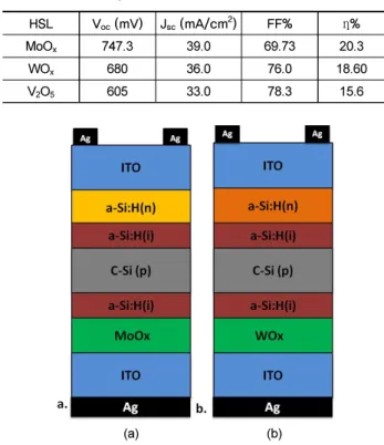
As discussed in literatures Light current voltage (LIV) data of different hole selective cells are shown in Table 1 1) .
p-type Si wafer: As described in literature, in case of p-wafer cells i-layer at front surface yields interface passivation. Sche- matics of (a) c-Si (p) / a-Si:H/ MoO x heterojunction solar cell structure and (b) c-Si(p)/a-Si:H/WO x heterojunction solar cell has been depicted in Fig. 3.
Transportation of holes at the back contact, through tunneling via intrinsic and hole extracting layer is significant to reduce barrier effects and better performance 21) . For n-type wafer, the thicker top a-Si (i) layer results in a lower short circuit current whereas, in case of p-wafer cell front i-layer should be as thick as 50 nm (approx) so that top layer generates high electric field that results in accumulation of carriers originated by short wavelength light 22) .
As reported in literatures hole extracting materials can serve as both p-type replacement and additional contact layer to assist hole extraction 23) . The analysis revealed if MoO x and WoO x act as additional contact layers, the offset between ITO and
thickness of 200 µm . Consequently, standard RCA cleaning has been adapted for removal of organic/inorganic contaminants succeeded by HCl/HF dipping, rinsing in DI water and drying with nitrogen gas. The a-Si:H (i) layer of thickness 8 and 6 nm was deposited in both front and rear sides of C-Si respectively via cluster PECVD at 200°C. A n+ phosphorus doped layer of thickness 12 nm is also deposited in back side of device through PECVD. Likewise, MoO x 10 nm has been deposited on front side of device by thermal evaporation 25) . ITO is placed on front and back layers as of 100 nm and 80 nm by pulsed DC magnetron sputtering at 100°C. Silver (Ag) paste is screen printed as continuous metal on rear side and grid type on front side 26) . Lastly samples are cured at 160°C for 30 min in industrial belt furnace.
1.4 Material requirement
Eventually, recent investigations have reported carrier selective materials utilizing low thermal budget, superb separation of carriers and lower recombination velocity and insignificant contact resistivity 27) . These materials can be implemented as an alternative solution to silicon dopants. It has been reported in literatures that PEDOT:PSS have exhibited marvelous open-circuit voltage (V oc ) of 657 mV and conversion efficiency more than 20% 27-28) . But it shows chemical instability due to its hygroscopic character which leads to severe device degradation.
TMOs are a kind of material that possess excellent carrier- selective properties. The use of TMOs as p-type emitters in n-type c-Si has also been investigated for MoO 3 , WO 3 and V 2 O 5
demonstrating a potential conversion efficiency of 22.5%, 12.5% & 15.7% for this novel solar cell concept 28) . Molybdenum trioxide (MoO 3 ), tungsten trioxide (WO 3 ) and vanadium pentoxide (V 2 O 5 ) are some examples of hole extracting TMOs which can replace p type silicon dopants in HIT structures. TMOs possess large work function. These TMOs work as hole-selective contacts as they show high work functions (>5 eV) and lie very nearer to the High Occupied Molecular Orbital (HOMO) level of p-type organic semiconductors, which support ohmic contact origination.
(a) (b)
Fig. 3. Schematics of the (a) C-Si (p) / a-Si:H/ MoO
x
and (b) C-Si(p)/
a-Si:H/WO
x
heterojunction solar cell structure
(4)
2. Factors affecting HIT cell performance
n-type Silicon wafer: Majority of high efficiency HIT cells have been fabricated by considering n-type C-Si wafer as base material. Even though it is possible to fabricate HIT cells on p-wafer, still V oc is inferior as compared to n-wafer cells as depicted in Fig. 4 29) . Reports say faster recombination rate of p-type wafer would lead to this issue 30) .
Hole extracting layers: As reported in literature, amorphous silicon (a-Si) doped layers suffer from optoelectronic losses, complexities and deposition as it requires PECVD which introduces toxic gases, require explicit control to optimize proper V oc and J sc. and quite costly deposition methods 30) .
Moreover, the doping technique comprises high cost, high temperature treatments (more than 800°C), tiny contact fractions, removal of boron rich layer and junction removal 30-31) .
3. Temperature dependency of carrier selective HIT
The insertion of i-layer in carrier selective cells creates large valance band offset energy 31) . Drift diffusion velocity of i-layer hinder transfer of holes due to large valance band offset energy.
This property enhances with increased forward bias voltage and enhance transmission of minority carriers i.e holes from C-Si base to carrier selective layers 31) . This property opposes enhanced dark current that turned into lower dependence of carrier selective cells on temperature.
4. Effect of work function on cell
The work function ( ψ) of hole selective material shows remarkable impact on the heterocontact characteristics of device and plays crucial role in determining the charge transport as well as contact resistance behavior 31) .
Work function decides transportation mechanism of holes.
The potential barriers for electrons depend on work function of hole selective material 32) . For an efficient hole selective cell height of electron barrier should be higher and height of hole barrier should be lower for efficient transportation of holes 32) . As work-function decreases electron barrier height also decreases which leads to inefficiency of cell 32-33) .
For work function below 4.5 eV no remarkable band bending occurs and simultaneously V oc decrease. Decreasing work function increases barrier height for holes 33) . Thus, value of work-function transported nearby interface which leads to assembly of electrons near interface between hole selective and i layer resulting into increased recombination. This strongly effect V oc , FF and ƞ 34) . Thus work-function of hole extraction material should be high.
5. Effects on HIT cell parameters
V oc is an important cell parameter and can be conveyed as V oc = kT/q ln (I sc /I 01 ). Leakage current is indirectly proportional to V oc . Therefore with increasing leakage current I o1 , V oc
decreases. Thickness of emitter does not control V oc. until the thickness goes beyond 27 nm 34-35) . Increased thickness escorts to lowering of blue response of the QE and Jsc which leads to use of thinner p emitter. It has also been investigated that proper surface texturing and improved passivation are the two
(a)
(b)
Fig. 4. J-V curve for MoO
x
contact based on (a) n-wafer (b) p-
wafer
(5)
This work focuses on HIT employing hole selective material to replace boron doped layer. These devices have shown the potential to challenge the conventional HIT cells. It can be fabricated on both n-type and p-type. While implementing on n-base with hole extracting layer as emitter and n+ as BSF it shows higher efficiency as compared to p-base. HIT cells impose lower thermal budget and faster fabrication process. At the same time carrier selective HIT cells has lower dependency on temperature, evolving as a risk-free materials to be deposited alternative to p / n doped a-Si:H. These devices depict wide band gap with a distinctive p- or n-type character and a broad range of work functions varying from 2 to 7 eV. For hole selective contacts work-function has to be higher i.e in the range of 4 - 7 eV. In order to achieve best cell results proper surface texturing and improved passivation are the two major factors which control V oc . J sc depends on thickness of emitter layer, absorption by wafer, BSF structure and modified surface passivation.
Acknowledgement
This work is supported by the Korea Institute of Energy Technology Evaluation and Planning (KETEP) and the Ministry of Trade, Industry and Energy (MOTIE) of the Republic of Korea (No. 20173010012940).
References
1. S. M. Iftiquar, Y. S. Lee, V. A. Dao, S. H. Kim and J. S. Yi,
“High efficiency Heterojunction with intrinsic thin layer solar cell: A short review,” Materials and processes for energy and processes for energy: communicating current research and tech- nological developments, pp. 59-65, 2013.
2. K. Wakisaka, M. Taguchi, T. Sawada, M. Tanaka, T.
Matsuyama, T. Matsuoka, S. Tsuda, S. Nakano, Y. Kishi, Y.
Kuwano, “More than16% solar cells with a new ‘HIT’ (doped a-Si/nondoped a-Si/crystalline Si) structure,” Photovoltaic Specialists Conference, pp. 887-892, 1991.
3. M. Tanaka, S. Okamoto, S. Tsuge, S. Kiyama, “Development of HIT solar cells with more than 21% conversion efficiency
Kenichiro, T. Shinya, N. Shoichi, High-efficiency a-Si/c-Si Heterojunction solar cell. 1st World Conference on Photovol- taic Energy Conversion (Hawaii), pp. 1219-1226, 1994.
6. B. Jagannathan, W. A. Anderson, J. Coleman, “Amorphous silicon/p-type crystalline silicon Heterojunction solar cells,”
Solar Energy Materials and Solar Cells, Vol. 46, pp. 289-310, 1997.
7. M. W. V. Cleef, F. A. Rubinelli, R. Rizzoli, R. Pinghini, R. E.
I. Schropp, W. F. V. D. Weg, “Amorphous Silicon Carbide/
Crystalline Silicon Heterojunction Solar Cells, A Comprehensive Study of the Photocarrier Collection,” Jpn. J. Appl. Phys., Vol.
37, pp. 3926-3932, 1998.
8. N. Jensen, U. Rau, R. M. Hausner, S. Uppal, L. Oberbeck, R.
B. Bergmann, J. H. Werner, “Recombination mechanisms in amorphous silicon/crystalline silicon Heterojunction solar cells,”
J. Appl. Phys., Vol. 87, pp. 2639-2645, 2000.
9. J. Damon-Lacoste, P. R. Cabarrocas, P. Chatterjee, Y.
Veschetti, A. S. Gudovskikh, J. P. Kleider, P. J. Ribeyron,
“About the efficiency limits of Heterojunction solar cells,” J. of Non-Cryst. Solids, Vol. 352, pp. 1928-1932, 2006.
10. T. Mishima, M. Taguchi, H. Sakata, E. Maruyama, “Develop- ment status of high-efficiency HIT solar cells,” Solar Energy Materials & Solar Cells, Vol. 95, pp. 18-21, 2011.
11. A. Kanevce, W. K. Metzger, “The role of amorphous silicon and tunneling in Heterojunction with intrinsic thin layer HIT solarcells,” J. Appl. Phys., Vol. 105, 094507, 2009.
12. M. Schmidt, L. Korte, A. Laades, R. Stangl, C. Schubert, H.
Angermann, E. Conrad, K. V. Maydell, “Physical aspects of a-Si:H/c-Si hetero-junction solar cells,” Thin Solid Films, Vol.
515, pp. 7475-7480, 2007.
13. T. Mishima, M. Taguchi, H. Sakata, E. Maruyama, “Development status of high-efficiency HIT solar cells,” Solar Energy Materials
& Solar Cells. Vol. 95, pp. 18-21, 2011.
14. J. Geissbühler, J. Werner, S. M. de Nicolas, L. Barraud, A.
Hessler-Wyser, M. Despeisse, S. Nicolay, A. Tomasi, B.
Niesen, S. De Wolf, C. Ballif, “22.5% efficient silicon Hetero- junction solar cell with molybdenum oxide hole collector,”
Applied Physics Letters, Vol. 107, 081601, 2015.
15. C. Battaglia, S. M. de Nicolás, S. De Wolf, X. Yin, M. Zheng, C. Ballif, A. Javey, “Silicon Heterojunction solar cell with pas- sivated hole selective MoOx contact,” Applied Physics Letters, Vol. 104, 2014.
16. M. L. Yu, Y. L. Hsieh , S. K. Jou, T. T. Li, C. C. Lee, “Investi-
gation of intrinsic hydrogenated amorphous silicon (a-si:H)
(6)
thin films on textured silicon substrate with high quality passi- vation,” IEEE China semiconductor technology international conference (CSTIC), 2017.
17. M. Bivour, J. Temmler, H. Steinkemper, M. Hermle, “Moly- bdenum and tungsten oxide: High work function wide band- gap contact materials for hole selective contacts of silicon solar cells,” Solar Energy Materials & Solar Cells, pp-34-41, 2015.
18. J. Bullock, A. Cuevas, T. Allen, C. Battaglia, “Molybdenum oxide MoOx: A versatile hole contact for silicon solar cells,”
Applied Physics Letters, Vol. 105, 232109, 2014.
19. J. Bullock, D.Yan, A. Cuevas, Y. Wan, C. Samundsett, “n- and p-type silicon solar cells with molybdenum oxide hole con- tacts,” Energy Procedia, Vol. 77, pp. 446-450, 2015.
20. C. Messmer, M. Bivour, J. Schön, S. W. Glunz, M. Hermle,
“Numerical Simulation of Silicon Heterojunction Solar Cells Featuring Metal Oxides as Carrier-Selective Contacts,” IEEE Journal of Photovoltaics 1, 2156-3381, 2018.
21. R. M. Swanson, “Approaching the 29% limit efficiency of sili- con solar cells,” in Proc. 31st IEEE Photovolt. Spec. Conf. Lake Buena Vista, Lake Buena Vista, FL, USA, 2005, pp. 889-894 22. P. Wurfel, U. Wurfel, Physics of Solar Cells: From Basic
Principles to Advanced Concepts, 3rd ed. Weinheim, Germany:
Wiley, 2016
23. L. G. Gerling, S. Mahato, A. Morales-Vilches, G. Masmitja, P.
Ortega, C. Voz, R. Alcubilla, J. Puigdollers, “Transition metal oxides as hole-selective contacts insilicon Heterojunctions solar cells,” Sol. Energy Mater. Sol. Cells, Vol. 145, pp. 109-115, 2016.
24. M. Bivour, J. Temmler, H. Steinkemper, M. Hermle, “Moly- bdenum and tungsten oxide: High work function wide band gap contact materials for hole selective contacts of silicon solar cells,” Sol. Energy Mater. Sol. Cells, Vol. 142, pp. 34-41, 2015.
25. J. Bullock, Y. Wan, M. Hettick, J. Geissbühler, A. J. Ong, D.
Kiriya, D. Yan, “Survey of dopant-free carrier-selective con- tacts for silicon solar cells,” in Proc. 2016 IEEE 43rd Photovolt.
Spec. Conf., pp. 210-214, 2016.
26. M. Bivour, C. Messmer, L. Neusel, F. Zähringer, J. Schön,
“Principles of carrier-selective contacts based on induced junc- tions,” in Proc. 33rd Eur. PV Solar Energy Conf. Exhib., Amsterdam, The Netherlands, Sep. 25-29, pp. 348-352, 2017.
27. L. Neusel, M. Bivour, M. Hermle, “Selectivity issues of MoOx basedhole contacts,” Energy Procedia, Vol. 124, pp. 425-434, 2017.
28. M. Bivour, F. Zahringer, P. Ndione, M. Hermle, “Sputter-de- posited WOx and MoOx for hole selective contacts,” Energy Procedia, Vol. 124, pp. 400-405, 2017.
29. H. Mehmood, H. Nasser et al., “Simulation of an efficient sili- con heterostructure solar cell concept featuring molybdenum oxide carrierselective contact,” Wiley Energy Research, 2017.
30. E. Centurioni, D. Iencinella, R. Rizzoli, F. Zignani, Silicon Heterojunction Solar Cell: A New Buffer Layer Concept With Low-Temperature Epitaxial Silicon. IEEE Trans. Elec. Dev.
Vol. 51, pp. 1818-1824, 2004.
31. S. D. Wolf, M. Kondo, “Abruptness of a-Si:H/c-Si interface re- vealed by carrier lifetime measurements,” Appl. Phys. Letts., Vol. 90, 042111, 2007.
32. Fujiwara H., Kondo M., “Impact of epitaxial growth at the het- erointerface of a-Si:H/c-Si solar cells,” Appl. Phys. Letts., Vol.
90, 013503, 2007.
33. H. Fujiwara, M. Kondo, “Effects of a-Si:H layer thicknesses on the performance of a-Si:H/c-Si Heterojunction solar cells,” J.
Appl. Phys., Vol. 101, 054516, 2007.
34. F. Einsele, P. J. Rostan, M. B. Schubert, U. Rau, “Recombina- tion and resistive losses at ZnO/a-Si:H/c-Si interfaces in Heterojunction back contacts for Si solar cells,” J. Appl. Phys.
Vol. 102, 094507, 2007.
35. Y. Xu, Z. Hu, H. Diao, Y. Cai, S. Zhang, X. Zeng, H. Hao, X.
Liao, E. Fortunato, R. Martins, “Heterojunction solar cells with n-type nanocrystalline silicon emitters on p-type c-Si wa- fers,” J. Non-Cryst. Solids, Vol. 352, pp. 1972-1975, 2006.
36. Y. J. Song, “Anderson W A, Amorphous silicon/p-type crys- talline silicon Heterojunction solar cells with a microcrystalline silicon buffer layer,” Solar Energy Mat. Sol. Cells, Vol. 64, pp.