Vol.14, No.6, pp.74-78 (2020)
Design Method and Analysis for Current Limit Charger of Battery System for Regulating CDE Power of Satellite
Kyudong Kim1,†
1Korea Aerospace Research Institute
Abstract
The cooler driver electronics (CDE) for maintaining a low temperature of a satellite payload IR sensor has a compressor with a pulsation current load when in operation. This pulsation current creates a large voltage fluctuation and may negatively affect both the load and regulated bus stability. Thus, a CDE power conditioning system has a battery for use as a buffer that is connected in front of the CDE load line. In this system, a battery charger limiter circuit is required to protect from an over-charge of the battery and power to the load. In this study, an optimal design and parameter selection were developed and simulated.
Key Words: Satellite, Payload Powering, Cooler Drive Electronics, Battery System, Current Limit Charger
1. Introduction
Cooler drive electronics (CDE), which are used to keep the IR sensor, payload on a satellite, drives the compressor to maintain low temperatures [1] and the pulse-type load current generated when the compressor is operated causes a large voltage fluctuation at the load input, thereby affecting the stability of the regulated 28V bus power source in the power control distribution system. Therefore, for a stable power supply of CDE units and the stability of satellite-controlled buses, the CDE power conditioning system uses batteries for buffering separately from those for the main body. In this system, charging is carried out using a battery charger limiter circuit to apply the functions of controlling the charging current of the battery and supplying power to the load.
Because current limiting circuits have functions for preventing a battery current overcharge and maintaining a constant current charge, the circuit selection and parameter design are extremely important. In this study, the optimal design and parameter selection of a battery charger limiter circuit were carried out and the adequacy of the CC charging and load power supply and variation width of the load supply voltage was verified through an analysis using the modeled battery and compressor load [1].
1.1 Configuration of the CDE power conditioning system
As shown in the block diagram in Fig. 1, the CDE power conditioning system consists of a power conditioning and distribution unit (PCDU), an 28V regulated bus power distribution unit (28VPD), an onboard computer (IBMU), an IR power distribution unit (IPDU), a CDE battery, and a cooling driver electronics (CDE). The IR power distribution unit consists of fuses for protecting an over-current of the cooling motor load, a cut-off relay for circuit switching and protection, and a current-limited charging circuit that supplies power to the load at the same time as charging the battery, and a diode to prevent reverse current [2].
Because the CDE operates at on/off pulses between 70–100 Hz, buffers such as batteries, capacitors, or a regulation converter are needed to stabilize the regulated bus. When using the capacitor method, a minimum capacitance of 50 mF is required to stabilize the regulated bus, which is not a suitable method for satellite systems with limited weight requirements, as the mass is 4-times and size is 3-times as large as when using a battery. In addition, the 50 mF capacitor is approximately 60-times 800 μF, the bus filter capacity used for regulated buses, resulting in a downside of an initial large value of the inrush current and requiring a separate circuit to cope with and initially charge it. In the case of the regulation converter, owing to the development period and cost issues, the final choice was to select a 7s8p structure Li-ion battery with the heritage design of the K3A satellite.
Received: Apr. 28, 2020 Revised: Aug. 05, 2020 Accepted: Aug. 05, 2020
† Corresponding Author
Tel: +82-42-860-2304, E-mail: [email protected]
Ⓒ The Society for Aerospace System Engineering
PCDU
28VPD
IPDU
CDE Battery 28VPC
J2 (Battery)
J3 (Relay Outputs)
J1 (Power & Signal)
+ -
AD590
CDE RED
J5 (Commands)
IBMU Analog TLM Bi-level TLM
Voltage TLM J6 (Telemetries)
Regulated 28V Bus 27.5~28.5 [V]
28V
Regulator Bus Bar LCL J1 (Power)
+
- J7 (Fuse)
J7 (Fuse) CDE PRI
Fig. 1 Block Diagram of CDE Power Conditioning System
1.2 Equivalent Circuit of CDE Power Conditioning System
CDE power conditioning systems using batteries can be represented as shown in Fig. 2, with a 28V regulated bus power, diodes to prevent reverse current, CDE batteries and equivalent circuits simplified by load. The load used here can be modelled as a pulse-type load that is turned on/off at 100 Hz intervals, as expressed in Fig. 2, and the battery can also be modelled through the equivalent impedance model [3].
Regulated Bus (27.5~28.5V)
CDE Load (100Hz, 100Wmax)
Fig. 2 Block Diagram of CDE Power Conditioning System
The battery used in this system is a lithium-ion battery consisting of a structure of the 7s8p of 18650 Sony cells, with 56 cells and a name plate capacity of 12Ah.
For verification of the design, the battery was subjected to an AC impedance model consisting of R-L-C, as shown in Fig.
3, and the analysis was conducted by applying an AC impedance at the end of life, which considered 100% SoC, beginning of life at 20°C conditions, 30% capacity fade, and 1 string failure, as provided by the manufacturer [4, 5].
Fig. 3 AC Cell Impedance Model of CDE Battery
2. Interpretation of Charger Limiter Circuit
Current limit chargers inside the IR power distribution units placed for limiting the battery charge current and load power supply of the CDE power supply systems may consist of circuits that determine the driving area of the FET by sensing the load line current, as shown in Fig. 4. This is a circuit in which the gate voltage is regulated according to the load current, and when a current above the set limit current flows, the FET operates in the active region, limiting the drain current [6–8].
1k 28V_Bus
Bus Bar
RTrip
Load
GND RBias2 RBias1
IREF
VA
IG
IE IB IL
ICH1 VB
RSense
VCC Vdrop
+ - VEB_H1
VEB_H2+
- VG
ICH2 VT
Fig. 4 Current Limit Charger with Cascode Mirror 2.1 Charger Limiter Circuit Selection
A separate charging circuit is required to prevent overcharging and limit the charging current of CDE batteries.
A passive method using resistance can be used to limit the current but is not a suitable method for a CDE operation because it results in decreases in voltage and efficiency owing to loss of flow. Possible active control methods can be divided into the load side switch control method or the method of charging through CC-CV control using a DC-DC converter.
Because the batteries used in this system play the role of damping for a stable power supply and bus power protection, the DC-DC converter is an excessive design and conflicts with the reasons for selecting the batteries as described in Section 1.1. Therefore, this system uses the method of controlling the load side switch with a charger limiter circuit. In the case of the inrush current limiter, which limits the current through commonly used load side FETs, the transient current is limited using an N-Channel or p-Channel MOSFET. However, it is difficult to precisely match the limiting current required by the battery through this approach because there is no current sensing circuit [9, 10]. Therefore, in this study, circuits where the current sensing circuit on the load side exists, as shown in Fig. 4, were selected to satisfy the 3.8A charging current,
Internal
Resistance Series Inductance
Shunt Capacitance
Z
X R
Inductance
Capacitance θ
Resistance
which is a design requirement of a CDE battery system. This circuit uses the heritage design used in LCL circuits for the power distribution channels of the satellites, and only the current limiting function was utilized in the CDE battery systems [8].
2.2 Current Limit Circuit in the Current Mirror Type
Current mirror type current limit circuits have a constant bias current formed by the sinking mirror at the bottom and a voltage difference caused by the bias current difference generated by the source mirror at the top, and this changes the gate voltage VT of the load side p-MOSFET to perform this control. If the current is less than or equal to the set limit current, the gate current will be larger than or equal to Vsg(th)
and thus the load switch will operate at the Ohmic region, and if the current is greater than the limit current, the gate voltage will be less than Vsg(th), and will operate within the active region and the current will be limited to a constant degree.
The RMS value of the load current required by the current system is 3.57A and the limit range of the current to protect the load over-current is set to 3.8A.
For the utility of the design and the stable operation of the NPN transistor, the bias current of the sinking mirror circuit is set to 1 mA to select the resistance. Eq. (1) below obtains a resistance satisfying the set bias current.
For the utility of the design and the stable operation of the NPN transistor, the bias current of the sinking mirror circuit is set to 1 mA to select the resistance. Eq. (1) below is used to obtain a resistance that satisfies the set bias current.
=−− 2 ×
3 × + ≈ 1 (1) Here, Vdrop indicates the size of the voltage drop caused by sensing resistance when setting the 3.8A limit current, and the current system has the sensing resistance set to 25 mΩ. A large sensing resistance can increase the accuracy when selecting RTrip, but if too large it can cause a voltage loss owing to a line drop, and if too small it can reduce the sensing sensitivity.
Here, VCEsat is negligible in the operation of a mirror circuit, and RTrip is negligible because it is extremely small compared to the bias resistance Rbias2. The base-emitter voltage was assumed to be 0.7V, the typical transistor design voltage.
Therefore, Rbias2 is calculated to be 9.06 kΩ according to Eq.
(1) and the above conditions, and was determined to be 9.09 k, which is a selectable resistance value in an actual supply.
2.3 Designing and Selecting Limiting Current Parameters
The limiting current is determined by a combination of the sensing resistance (Rsense) and trip-off resistance (RTrip), and based on the sensing resistance values proposed in Section 2.1,
the trip-off resistance can be obtained using Eqs. (2) and (3) below. The two formulas below can create the operating conditions for the circuit in the top sinking mirror, where if the current value on the load side through the sensing resistance is more than or equal to the desired set current value, the voltage decrease due to the sensing resistance reaches the emitter-base saturation voltage of the transistor owing to the voltage drop in VA and VB, and the upper circuit acts as a mirror. Therefore, because this shows the same collector current, the gate current on the load side FET is limited and the voltage on the gate does not satisfy the threshold voltage and operates in the active region.
_= − > (2)
_= −
= (− × ) − − × > (3) According to the equation above, the trip-off resistance resulting in a mirror operation owing to the transistor saturation voltage formation is 95 mΩ.
The following equations can be used to check the gate current and voltage in normal and trip-off modes. The threshold voltage of the gate voltage is generally designed to be approximately 7V and requires a value of more than or equal to 10V considering the parasitic component of the gate driving circuit or the margin of the element.
= + (4)
= × (5) In normal mode, because the BJT in the top sourcing mirror circuit does not operate in the saturated area, a gate voltage of approximately 18V is applied owing to the voltage drop by the collector current (IL ≈ IREF) which is equal to the mirror current formed by the bottom sinking mirror circuit, with an approximately 1 mA bias current. This causes the source-gate voltage of the load side p-MOSFET to establish a voltage above the threshold voltage and operate in the ohmic region.
During an active region operation, the collector current (ICH1) changes owing to the transconductance variation, and when the VEB voltage decreases the ICH1 current decreases as well.
Here, when load current is reduced, the PNP BJT at the top of the cascode reaches the OFF region and the collector current ICH1 approaches zero. At this point, the gate current IG
gradually reaches the lower mirror current size and ultimately operates as IG≈IL≈IREF.
In trip-off mode, the gate current (IG) is extremely small owing to Eq. (4) because the sourcing mirror circuit at the top also operates in the transistor saturated area to form a mirror current. By Eq. (5), the VEB voltage is increased owing to the collector current increase, and thus the gate voltage is approximately 22 V or higher, and the source-gate voltage of
the load side p-MOSFET is below the threshold voltage and operates in the active region.
3. CDE Battery System Interpretation
Fig. 5 Simulation Schematic for Current Limit Charger
For an interpretation of the battery charger limiter circuit for the power supply of the payload CDE, the TINA-TI Spice simulation tool was constructed, as shown in Fig. 5, and FET ON/OFF control signals were added for operation verification, although they do not exist in the actual circuit. In changing the load resistance, the operation of the current limit according to the load current size as well as the main current and gate voltage of the mirror circuit were checked. For a trip-off resistance, the simulation was conducted by adding the ON/OFF control circuit at the bottom and setting the resistance value to 103Ω to carry out the 3.8A limit considering the parasitic elements of circuit.
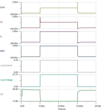
3.1 Normal Mode Operation
To verify normal mode operation, the load is set to a simple resistance load of 10Ω, and the load current is set to below 3.8A, which is the set trip-off level, and thus no current limit operation occurs. Fig. 6 shows the simulation results under the normal mode load. This condition is actually operated in CV mode charging a CDE battery in on-orbit operation of satellite.
If the bias resistance is set to 9.09 kΩ, as determined in Section 2.1, it can be seen from waveforms 2 and 3 of Fig. 6 that the bias current is approximately 1 mA.
The collector current (ICH1) in the upper sourcing mirror circuit changes as the load current changes, the load current is approximately 2.78A under the 10Ω load identified in this simulation, at which time the collector current (ICH1) is
measured to be 470 μA.
Fig. 6 Simulation Results for Normal Mode
Because the bottom sinking mirror circuit is equal to the bias current by the current mirroring, the gate current is measured using Eq. (4) as the difference between the bias current and the collector current. The gate voltage is measured at approximately 17.79 V, and thus the source-gate voltage of the Load Side p-MOSFET has a voltage over the applied threshold voltage and thus can be verified to operate in the ohmic region.
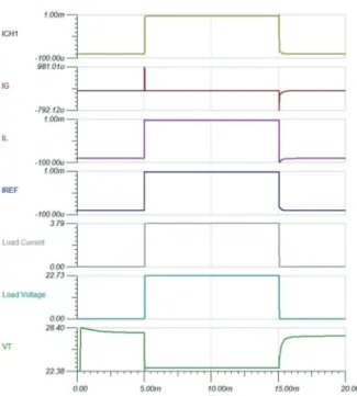
3.2 Current Limit Mode Operation
To check the current limit mode operation, the load is set to a simple resistive load of 6Ω and the load current is greater than the set trip-off level of 3.8 A, which results in a current limit. Fig. 7 shows the simulation results at the current limit mode load.
The biggest difference between the current limit mode and normal mode operation is the collector current (ICH1) in the top sourcing mirror circuit, which can be seen from the first waveform of Fig. 7 to have a value of approximately 1 mA by the current mirroring. The gate voltage, the fifth waveform of Fig. 7, is measured at approximately 22.83 V, which confirms that the source-gate voltage of the load side p-MOSFET is below the threshold voltage and operates in the active region.
This can also be further confirmed through the fourth waveform of Fig. 7, where the p-MOSFET operating in the active region fails to fully turn-on and the voltage applied to the load is measured at 22.725 V because of the drop in the drain-source voltage (VDS) owing to the amplification ratio of the FET element.
Fig. 7 Simulation Results for Current Limit Mode
4. Conclusions
In this paper, the main parameters of the current limiter charger circuit of battery power conditioning systems used for supplying power to payloads were selected and verified through analysis and interpretation. The mirror circuit was used to determine the set limit current considering the characteristics of the load and the battery limiting current, and the operating area of the load side switch was determined through the voltage drop due to the set resistance.
In this topology, if the load current becomes smaller, the bias current in the mirror circuit will also become smaller, thereby causing the bias current to change owing to the load variation. This results in changes in the load side p-MOSFET gate voltage and limiting the current level. For example, in the case of LCL level 3.8 A setting, even if the load current is 3.58 A, the collector current will reach 1 mA and the current will be limited. This exceeds the trip-off level tolerance specification of ±5% and does not satisfy the design criteria [6]. Thus, applying a fixed voltage to the base of the bottom NPN BJT type sinking mirror circuit could be a plausible alternative. In general, a static-voltage source is applied to a mirror circuit using a generator diode, but this method may be used for programs that require precision. For the topologies used by K3A satellites, the zener diode allows precise control of the charge limiting current size of the current limiting circuit. In future papers, a comparison between the topologies used in K3A and the topologies analyzed in this paper will be compared, and it will be verified whether the current limiting behavior is achieved according to the design in the actual FM
model.
References
[1] M. Mai, I. Ruhlich, A. Schreiter and S. Zehner, “AIM- Space cryocooler programs,” Cryocooler 16, ICC Press, Boulder, pp. 133-141, 2011.
[2] K. D. Kim, J. H. Yang, S. W. Park and J. C. Koo, “Design for stabilizing power of pulsated-current load CDE unit in satellite system,” SASE 2018 Spring Conference, April 2018.
[3] K. D. Kim, S. W. Park and J. C. Koo, “System simulation using BOL/EOL equivalent impedance model of CDE battery for satellite system,” SASE 2019 Spring Conference, P9-2, April 2019.
[4] M. Meyer, “KOMPSAT-7 CDE Battery Electrical Analysis Report,” Nov. 28, 2018.
[5] J. Troutman and S. Lamvert, “ABSL initial performant comparison f Sony 18650 hard carbon cell and Sony 18650 hard carbon mandrel cell,” 9th Annual International Energy Conversion Engineering Conference, 03 August, 2011.
[6] European Cooperation for Space Standardization, ECSS- E-ST-20C, Space Engineering, Electrical and Electronic, 15 April 2016
[7] European Cooperation for Space Standardization, ECSS- E-HB-20-20A, Space Engineering, Electrical and Electronic, 15 April 2016
[8] C. Delepaut, T. Kuremyr, M. Martin, F. Tonicello, “LCL current control loop stability design,” Proc. 10th European Space Power Conference, The Netherlands, 15–
17 April 2014
[9] Shi, H., Zhao, C., Jin, Y., and Liu, Y., “Current limiting protection in spacecraft power system,” ICEPE-ST, 2015.
[10] David, C. Salerno, “Self-latching current limiter,” United States Patent 4,835,649, May 30, 1989