DOI http://dx.doi.org/10.9725/kstle.2015.31.6.239
Effect of Brush Treatment and Brush Contact Sequence on Cross Contaminated Defects during CMP in-situ Cleaning
Hong Jin Kim†
Advanced Module Engineering, GLOBALFOUNDRIES, 400 Stone Break Road Extension, Malta, NY 12020, USA
(Received August 15, 2015; Revised October 9, 2015; Accepted October 10, 2015)
Abstract − Chemical mechanical polishing (CMP) is one of the most important processes for enabling sub-14 nm semiconductor manufacturing. Moreover, post-CMP defect control is a key process parameter for the purpose of yield enhancement and device reliability. Due to the complexity of device with sub-14 nm node structure, CMP-induced defects need to be fixed in the CMP in-situ cleaning module instead of during post ex-situ wet cleaning. Therefore, post-CMP in-situ cleaning optimization and cleaning efficiency improvement play a pivotal role in post-CMP defect control. CMP in-situ cleaning module normally consists of megasonic and brush scrub- ber processes. And there has been an increasing effort for the optimization of cleaning chemistry and brush scrub- ber cleaning in the CMP cleaning module. Although there have been many studies conducted on improving particle removal efficiency by brush cleaning, these studies do not consider the effects of brush contamination.
Depending on the process condition and brush condition, brush cross contamination effects significantly influ- ence post-CMP cleaning defects. This study investigates brush cross contamination effects in the CMP in-situ cleaning module by conducting experiments using 300mm tetraethyl orthosilicate (TEOS) blanket wafers. This study also explores brush pre-treatment in the CMP tool and proposes recipe effects, and critical process param- eters for optimized CMP in-situ cleaning process through experimental results.
Keywords − CMP, defect, post CMP cleaning, brush scrubber cleaning, process optimization
1. Introduction
Defect control is the most critical parameter in semi- conductor manufacturing for yield enhancement and device reliability [1-4]. And as scaling down to sub-14 nm, the device failure ratio by small particle is increased accordingly [1]. In the semiconductor pro- cess, chemical mechanical polishing (CMP) is known as the dirtest process to contaminate wafer surface and it is difficult to control post CMP defect. However, device feature size shrinkage and device complexity require more CMP steps in the manufacturing and post CMP defect control becomes more complicated. CMP process uses slurry chemical to make material surface
soften and abrarisve particle in slurry removes soften layer mechanically, which lead to global and local pla- narization of wafer [5]. And slurry chemical contains various polymeric additives for selectivity control and high material removal rate [5].
Hence, a lot of particles, organic materials and wear debris are generated during CMP process, such as abra- sive particle, abraded wafer material, polishing pad debris, and particles from the polisher itself [6-7]. And most of defects from CMP process are potentially con- sidered as yield-killing [1]. Examples of known device failure mechanism by non-metallic particle are shown in Fig. 1. Fig. 1 shows vertical structure of metal gate and contact patterning sequence schematically. Resid- ual slurry abrasive particle defect from metal gate CMP can influence on post contact patterning directly as shown in Fig. 1(a). And organic residue itself may not
†Corresponding author : [email protected] Tel: +1-518-305-1407, Fax: +1-518-305-6178
kill the device directly, however post process interact with organics and causes leakage failure as given in Fig. 1(b). Organic residue at post metal gate CMP pro- cess can be removed by contact etch process and it can be filled with metal contact material, which causes leakage failure between layers as shown in Fig. 1(b).
Historically, post CMP process has standalone ex-situ wet cleaning steps to remove CMP defects. However, device complexity and limitation of post CMP clean chemical make CMP process itself to remove CMP-
induced defects as much as possible. In order to min- imize post process defect, most CMP equipments have in-situ cleaning module in addition to polisher mod- ule. Depending on equipment maker, post CMP in-situ cleaning module is composed of megasonic cleaning, brush scrubber cleaning, high pressure fluid cleaning and their combination. And brush scrubber cleaning is known as the most efficient cleaning method in CMP cleaning module due to its physical force with direct contact between brush nodule and wafer surface [8-9].
A lot of researches and studies have been performed to enhance CMP in-situ cleaning efficiency. And most of post CMP cleaning efficiency reports have focused on brush scrubber cleaning and particle removal effi- ciency improvement by process optimization, brush properties and brush design [1, 6, 8-12]. However, contamination from brush itself to the wafer surface has not been investigated much. Inherently, brush itself contains a lot of particles inside and its cross contamination effect cannot be ignored. And this cross contamination directly influences on the particle removal efficiency and remain defects at post CMP process. In this paper, post CMP defectivity by brush scrubber cleaning is investigated. And experiments are focused on cross contamination effects in various pro- cess conditions.
2. Experiment
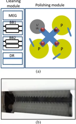
Reflection-LK polisher from Applied Materials Inc.
is used for the experiment. Schematic of the equip- ment is shown in Fig. 2(a). It is composed of 3 platens polishing module and in-situ cleaning module. And in- situ cleaning module is composed of megasonic tank, 2 brush scrubber boxes (brush box 1 (BB1) and brush box 2 (BB2)), and isopropyl alcohol (IPA) dryer. For this experiment, megasonic tank is not turned on because the purpose of this paper is to investigate brush cross contamination effect only. For the brush treatment effect on defectivity, new brush is imple- mented with and without brush treatment, and experi- ment wafers are run periodically. However, in order to investigate effect of brush gap and brush contact Fig. 1. Device failure mechanism by CMP-induced defects
at metal gate and contact patterning. (a) Abrasive particle: post metal gate CMP → dielectric material deposit → contact etch and abrasive defect block etch → ‘not open’ contact failure. (b) Organic residue particle: post metal gate CMP → dielectric material deposit → contact etch and organic residue etched at the same time (lateral open strucutre) → contact material deposit → leakage failure.
sequence on the defectivity, brush is used over 500 wafers polishing processed before experiment wafers run. The picture of brush module is given in Fig. 2(b).
Wafer is located in the middle of two brushes verti- cally. And both wafer and brushes rotate each other to remove wafer defects. Spray bars are installed above the brushes and chemical flows through spary bar. De- ionized water (DIW) flows through brush core to soak brushes. 300 mm tetraethyl orthosilicate (TEOS) blan- ket wafers are used for the experiment. The thickness of TEOS is 3k Å for all experimental conditions. And all TEOS wafers are processed cleaning module only without polishing process. Acidic based cleaning chemical is used for both brush scrubber boxes with 2000 ml/min flow rate at main cleaning step for all experiments. Brush and wafer rotation speed are 400
rpm and 50 rpm respectively. From the experiment, effect of brush soaking treatment, brush break-in, and brush contact sequence on the post defectivity are explored. After processing of brush cleaning, surface defects are inspected by SP3 tool from KLA-Tencor and defect types are classified by scanning electron microscopy (SEM) review. The SP3 inspection bin size is 60 nm.
3. Result and Discussion
Brush soaking effect on the cross contamination is summarized in Fig. 3. As described in experiment sec- tion, wafer is processed cleaning module only. Fig.
3(a) is the case of new brush implement with soaking treatment and Fig. 3(b) has no soaking process at brush implement. When a new brush is implemented in the CMP cleaning module, the brush condition is not completely ready-to-use state and it contains a lot of defects from brush manufacturing process. There- fore cross contamination is much worse than used brush. Fig. 3(b) shows post cleaning defect variation clearly. However, if brush is fully soaked in the CMP cleaning module before wafer process, its cross con- tamination effect can be improved a lot and results in defect variation improvement as shown in Fig. 3(a). In this paper, brush soaking process is defined as DIW flow with high flow rate through brush core for more than an hour before wafer processing. Brush soaking can soften brush sufficiently and it can remove con- Fig. 2. (a) Schematic of LK polisher. L/UL: loading-
unloading unit, H: head for wafer hold, P: platen (polishing pad, conditioner and slurry delivery arm), MEG: megasonic cleaning, BB1/2: brush box cleaning, DR: dryer, (b) Brush box cleaning module.
Fig. 3. Defect comparison with and without DIW soaking process. Wafer processed with CMP cleaner only. Brush soaking process case is (a) and non-soaked brush case is (b).
taminants inside brush. And it effectively minimizes cross contamination from new brush.
As shown in Fig. 3, new brush is unstable in defec- tivity and has high defect count, therefore brush needs to be properly treated in addition to brush soaking.
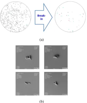
This process is called as brush break-in. In this paper, brush break-in is defined as 15 minutes cycling with one TEOS wafer and 25 TEOS dummy wafers pro- cessing followed by. This brush break-in effect on post defectivity is shown in Fig. 4(a). Left defect map is from the wafer processed without brush break-in and right defect map is from wafer run after brush break- in. As shown in the figure, dramatic defect improve- ment can be achieved by brush break-in. SEM review reveals that most of the defects are organic residue particle as shown in Fig. 4(b). Although the mecha- nism is not clearly undersood for brush break-in effect, insufficient brush wetting, brush nodule height varia- tion, nodule surface porosity and physical property, and contamination from brush manufacturing are sus- pected reasons for bad defect performance of new brush. And brush break-in treatment is considered to
overcome those incoming variations.
Brush gap is one the most important recipe variables to determine post CMP defectivity since the contact geometry determines the strength of particle removal force [6]. In this paper, brush gap is defined as dis- tance between the wafer surface and brush nodule.
Therefore, smaller brush gap indicates higher pressure to the wafer surface as shown in Fig. 5. Fig. 5 is sche- matic description of brush gap definition. And Fig. 6 shows brush gap effect on the post CMP clean defec- tivity. Considering incoming wafer qualities are same, -0.5 mm brush gap generates less defects than -1.5 mm brush gap case. Process recipe is composed of main clean, rinse, and ramp down steps for this exper- iment. Brush gap is controlled at main clean and rinse steps. When wafer moves to brush box, brush state is
‘open’ and immediately brush is closed to contact to wafer by set value of brush gap. Brush moving is oper- ated by mechanical motor. Although high contact pressure is favorable for particle removal as many lit- eratures has reported [7-8, 10], this result indicates that contamination from brush is more dominant at
Fig. 4. (a) Defect map before and after brush break- in and (b) SEM images of organic residue defect.
Fig. 5. Definition of brush gap. (a) positive number (or
‘open’), (b) 0, and (c) negative number (or ‘close’).
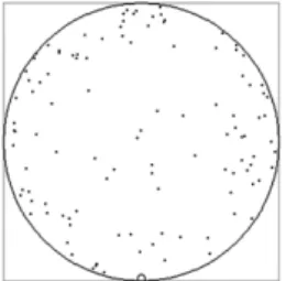
Fig. 6. Defect map after cleaning process. Brush gap condition is (a) -1.5 mm and (b) -0.5 mm. Total defect count of each map is (a) 333 and (b) 239.
higher contact pressure (or smaller brush gap) than particle removal on the post defectivity.
In addition to contact geometry, brush contact sequence is also important to cross contamination effect. Fig. 7 depicts schematic sequence of brush con- tact procedure. First case starts from ‘open’ step and touch the wafer immediately (‘close’ step) to set value of brush gap. This is called as ‘direct contact’ sequence which is shown in Fig. 7(a). The defect maps from Fig. 6 are from the direct contact sequence. In this case, defect map has always wafer edge signature and make brush mark across the wafer. This kind of defect signature is driven by brush touching with high down- force. However, contrary to the direct contact, so- called ‘soft-landing’ contact process has multiple steps (or ramp steps) between ‘brush open’ and ‘brush close’. At each ramp step, brush stays less than 2s and moves to the next step. This sequence is controlled by the process recipe and the brush movement is operated by motor. The advantage of soft-landing process is that brush touches wafer surface with weak down- force, therefore it can minimize brush touch effect.
The defect map with ramp step added (or soft-landing recipe applied) is given in Fig. 8. The main cleaning process recipe is same as the case of Fig. 6(a) after ramp steps. And it shows improved defectivity and weaker brush mark is observed than Fig. 6. Adding more ramp steps and gap optimization can further
improve post cleaning defectivity.
Experimental results in this paper address optimiza- tion of post CMP in-situ brush cleaning for advanced node semiconductor manufacturing. New brush is unstable at cross contamination aspect and it needs to be properly broken-in before actual wafer processing.
And brush cleaning recipe optimization can reduce cross contamination and maximize particle removal efficiency. Although this paper is focused on the brush cross contamination and brush stabilization, the results introduced in this paper can give insights on post CMP in-situ cleaning optimization.
4. Summary
Post CMP in-situ cleaning plays a critical role in yield enhancement and reliability of advanced node semiconductor manufacturing. And its importance is getting emphasized in the industry. As most CMP equipment accept brush scrubber cleaning in its clean- ing module, brush cleaning is the most effective method for particle removal. However, brush itself contributes to wafer contamination and it needs to be well treated to avoid cross contamination, in particular for the new brush. This treatment is called as brush break-in. Before wafer processing, fully soaked brush can minimize brush cross contamination and enough dummy wafers run improved post CMP cleaning defectivity. Experimental data in this paper well sup- ports brush break-in effect on defect reduction. Brush cleaning recipe determines contact sequence and par- ticle removal force. However, it also strongly influence cross contamination to the wafer surface. Therefore, both Fig. 7. Brush contact sequence. (a) Direct contact (open
→ main clean (closed)) and (b) soft-landing contact (open
→ ramp1 → ramp 2 → main clean (closed)).
Fig. 8. Defect map with ramp step added to the recipe used in Fig. 6(a). Defect count is 111.
particle removal efficiency and cross contamination should be considered at the same time to achieve opti- mized process condition. Slowly touched brush effec- tively reduces post defectivity. Although brush pre- treatment and cleaning process conditions can improve post in-situ brush cleaning defectivity, there are a lot of challenges to achieve further improvement.
References
[1] Kim, H. J., Lee, T. H., Qin, L., Kashyap, S. “Chal- lenges in post CMP in-situ cleaning for sub-14 nm device yield enhancement”, Proc. International Con- ference on Planarization/CMP Technology, pp. 230- 233, 2015.
[2] Ee*, Y. C., Tan, S. K., Chee, C. S., Tan, J. B., Zhang, B. C., Siew, Y. K., Tan, P. K., Zhang, F., Lai, K. H., Chettiar, M. S., Wang, X. B. Thomas Fu and L. C.
Hsia, “65 nm yield detractor caused by M1 filament shorts and solution”, Publications, PDF Solution (https://www.pdf.com/publications).
[3] Lariviere, S., Picore, F., Saez, P. L., Baltzinger, J.-L.
Delahaye, B., Matha, J., Gilhard, X., D'Oliveira, S., Lagarde, J. M., Prebot, J. L., Merlot, F., Nogueira, F., Petit, D., Williams, S., Besade, E., “Electro-static Induced Metal Breakdown at Interlayer Dielectric Post CMP Brush Clean Process”, Advanced Semi- conductor Manufacturing Conference, Berlin, Ger- many, May 2009.
[4] Kwark, H., Yang, W.-Y., Sung, I.-H. “Slurry particle behavior inside pad pore during chemical mechani- cal polishing”, J. Korean Soc. Tribol. Lubr. Eng., Vol. 28, No. 1, pp. 7-11, 2012.
[5] Steigerwald, J. M., Murarka, S. P., Gutmann, R. J.
Chemical Mechanical Planarization of Microelec- tronic Materials, pp.48-126, John Wiley & Sons, Inc., USA, 1997. (ISBN 0-471-13827-4)
[6] Kim, H. J., Bohra, G., Yang, H., Ahn, S.-G., Qin, L., Koli, D., “Study of the cross contamination effect on post CMP in-situ cleaning process”, Microelec. Engi,. Vol.
136, No. 25, pp. 36-41, 2015.
[7] Xu, K., Vos, R., Vereecke, G., Doumen, G., Fyen, W., Mertens, P. W., Heyns, M. M., Vinckier, C., Fransaer, J., “Particle Adhesion and Removal Mechanism during Brush Scrubber Cleaning”, J. Vac. Sci. Technol., B Vol. 17, 2284, 1999.
[8] Xu, K., Vos, R., Vereecke, G., Doumen, G., Fyen, W., Mertens, P. W., Heyns, M. M., Vinckier, C., Fransaer, J., Kovacs, F., “Fundamental Study of the Removal Mechanisms of Nano-sized Particles Using Brush Scrub- ber Cleaning”, J. Vac. Sci. Technol., B, Vol. 23, No.
5, pp. 2160-2175, 2005.
[9] Qi, Z., Lu, W., Lee, W., “A Novel Design of Brush Scrubbing in Post-CMP Cleaning”, Inter. J Machine Tools & Manuf., Vol. 85, pp. 30-35, 2014.
[10] Busnaina, A. A., Lin, H., Moumen, N., Feng, J.-W., Taylor, J. “Particle Adhesion and Removal Mecha- nism in Post-CMP Cleaning Process”, IEEE Trans.
Semi. Manuf., Vol. 15, No. 4, pp. 374-382, 2002.
[11] E-Eli, Y., Starosvetsky, D., “Review on Copper Chemi- cal-Mechanical Polishing (CMP) and Post-CMP Clean- ing in Ultra Large System Integrated (ULSI)-An Electrochemical Perspective”, Electroch. Acta, Vol.
52, pp. 1825-1838, 2007.
[12] Sun, T., Zhuang, Y., Li, W., Philipossian, A., “Investiga- tion of Eccentric PVA Brush Behaviors in Post-Cu CMP Cleaning”, Microelec. Engi., Vol. 100, pp. 20-24, 2012.