- 1436 -
평행평판 공진 해석과 효율적인 저감을 위한 모드 해석법과 모멘트 방법의 연구
신 은철*, 장 건호, 강 승택 인천대학교 정보통신공학과
Modal Analysis and MoM to Examine and Tackle Resonance Problems of Power/Ground Planes
Unchol Shin*, Gunho Jang, and Sungtek Kahng Dept. of Info. & Telecomm. Eng,, Univ. of Incheon
Abstract - In this work, we investigate the electrical and electromagnetic behaviors of the power-bus with a variety of shapes of aperture, on the signal integrity, using a rigorous methods(Modal or MoM) along with Modal analysis method.
1. 서 론
The power- and ground planes in PCBs are called the power-bus structure(PBS) and are known for causing cavity-mode resonance and possibly noise in the related system. T. Okoshi uses a modal sum expressions to characterize the structure[1]. Expanding the circuit concept, M. Hampe et al examines the effect of loads like DeCaps on the power-bus resonance[2]. Lately, C. Wang et al separately presented the performance of differential signaling in the power-bus and the advantage in reducing the number of resonance frequencies and impedance level[3]. Nevertheless, However, a question can be raised if the treatment such as DeCap placement, or differen-tial signaling will work properly well in the power-bus with a geometrical change like having slits shown in Z. Wang’s work or apertures.
2. 본 론
This study investigates the electrical and electro-magnetic behaviors of the power-bus with a variety of shapes of aperture, on the signal integrity, using a rigorous methods(Modal or MoM).
The slit power-bus structure can be modeled as a cavity having the PEC power- and ground planes and the PMC walls.
<Fig. 1> Top-view of a slit power-bus structure
Fig. 1 is the top-view of the power-bus structure where IPI1 is fed along the coaxial’s inner wire, passing the structure through the hole at (XPI1, YPI1). The output port is placed at (XPO, YPO).
Excluding the slit, the size of the power-bus is Wx×Wy×Wz. The sandwiched substrate is featured by Wz, 4.2 and 0.02 given as its thickness, relative di-electric constant and loss tangent[1-4]. With these parameters, rigorous evaluation methods are adopted, [1-4]. The modal analysis method goes with
(1) where
cmnii=cos(kxmXi)×cos(kynYi)×sinc(kxmPxi/2)×sinc(kynPyi/2) kxm=mp/Wx,kyn=np/Wy,w=2p f
1 2
0 ]
/ 2
[tan + −
= Wz
Q δ ωμκ
is 1 and 4 for (m =0, n =0) and (m≠0, n≠0) each. When (m≠0, n=0) or (m=0, n≠0),
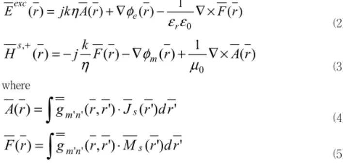
takes 2. tanδ, ε, μ, f, Pi and j denote loss-tangent, permittivity, permeability, frequency, port’s width and , respectively. Also, the method of Moment(MoM) is used to solve the MPIE which describes the power/ground plane structure.
) 1 (
) ( ) ( )
(
0
r F r
r A jk r E
r e
exc = +∇ − ∇×
ε φ ε
η (2)
) 1 (
) ( ) ( )
(
0
, kF r r Ar
j r
Hs+ =− −∇ m + ∇×
φ μ
η
(3)where
' )' ( )' , ( )
( r g
' 'r r J r d r
A = ∫ mn ⋅
s (4)
' )' ( )' , ( )
( r g
' 'r r M r d r
F = ∫ mn ⋅
s (5)
Eqns(2) and (3) denote scattered electric and magnetic fields. Plus, Eqns(2) and (3) are the magnetic and electric vector potentials. Ther wave numbers and intrinsic impedance of the medium are
0 0
μ ε
=
k ,
0
ε
0η
=μ
(6) The modal analysis method based on the cavity will be used to see the impedance profile of the geometry directly. As for the MoM’s simulations, we will check the physics of the apertures’ effects by following the current distribution.
Firstly, it will be demonstrated that the optimally chosen values of (Wx_Left, Ls, X0, Y0 ) or (Wx_Left, Ls, X0, Y0 and Wy_Left) are found to suppress to suppress resonance (1,0)-mode at 350MHz that occurs to the rectangular PBS with (Wx= 200mm, Wy= 150mm, Wz = 1.5mm).
2008년도 대한전기학회 하계학술대회 논문집 2008. 7. 16 - 18
- 1437 -
<Fig. 2> PBS’s resonance reduced from the original geometry toward the modified structure with the optimal position and size.
The optimal values turn out 188.77mm, 74.08mm, 179.33mm and 18.88mm as Wx_Left, Ls, X0 and Y0, respectively. Using the optimized slit enables the PBS to damp the 350MHz-resonance that is inherent in the regular PBS. The reduction amounts to 35dB.
Next using the MoM, we are about to watch how the surface current density is distributed with respect to the different apertures in the top plate of the power/ground planes. There will be one narrow slit and a loop formed along the lower edge and around the center, respectively.
(a) A narrow slit at the center of the lower x-axis
(b) An aperture loop around the center of the top plate
<Fig. 3> TTwo different cases of the apertures in the geometry
2 different slots are characterized by the MoM, to see the current density distribution. The feeder is located at the (0,0)-point and simulation is done with 380MHz.
0.0 0.5 1.0 1.5 2.0 2.5 3.0 3.5
0.02 0.040.060.080.100.120.14 0.00
0.02 0.04 0.06 0.08
Surface current density
X-axis Y -a
xis
0.0 0.5 1.0 1.5 2.0 2.5 3.0
0.00 0.02 0.040.06 0.080.10 0.120.14 0.01
0.02 0.03 0.04 0.05 0.06 0.07 0.08 0.09
Surface current density
X-axis Y -a
xis
(c) Jx of case 1 (d) Jy of case 1
0.0 0.5 1.0 1.5 2.0 2.5 3.0
0.000.020.040.060.080.100.120.14 0.01
0.02 0.03 0.04 0.05 0.06 0.07 0.08 0.09
Surface current density
X-axis Y-a
xis
0.0 0.5 1.0 1.5 2.0 2.5 3.0
0.0 0.5 1.0 1.5 2.0 2.5 3.0 3.5
0.020.040.060.080.100.120.14 0.00
0.02 0.04 0.06 0.08
Surface current density
X-axis Y-axis
0.0 0.5 1.0 1.5 2.0 2.5 3.0
(c) Jx of case 2 (d) Jy of case 2
<Fig. 4> Surface currents(Jx and Jy) with Fig. 3 Even in the non-resonance point, the field propagatesfrom the feed and induces currents maximize at the edges. Two cases have Jx top and bottom X-axes. The slot loop has lower Jy than case 1.
3. 결 론
The apertures and the influence are rigorously analyzed, revealing the EMI source and how to treat them
[참 고 문 헌]
[1] T. Okoshi, "Planar Circuits for Microwaves and Lightwaves", Berlin, Germany: Springer-Verlag, 1985.
[2] M. Hampe and S. Dickmann, "The impact of decoup-ling capacitors on the impedance of rectangular PCB power-bus structures", in Proc. 16th EMC Zurich, Switzerland, pp.251-256, 2005
[3] C. Wang, et al, "Coupling between differential sig-nals and the DC power-bus in multiplayer PCBs", IEEE Trans. EMC, Vol. 28, no. 2, pp. 337-345, 2005