pISSN 2288-3274
Light Trapping in Silicon Based Tandem Solar Cell:
A Brief Review
Sk Md Iftiquar
1)․ Hyeongsik Park
1)․ Vinh Ai Dao
1)․ Duy Phong Pham
1)․ Junsin Yi
1,2)*
1)College of Information and Communication Engineering, Sungkyunkwan University, Suwon, 16419, Republic of Korea,
2)Department of Energy Science, Sungkyunkwan University, Suwon, 16419, Republic of Korea
ABSTRACT: Among the various types of solar cells, silicon based two terminal tandem solar cell is one of the most popular one. It is designed to split the absorption of incident AM1.5 solar radiation among two of its component cells, thereby widening the wavelength range of external quantum efficiency (EQE) spectra of the device, in comparison to that of a single junction solar cell. In order to improve the EQE spectra further and raise short circuit current density (J
sc) an optimization of the tradeoff between the top and bottom cell is needed. In an optimized cell structure, the J
scand hence efficiency of the device can further be enhanced with the help of light trapping scheme. This can be achieved by texturing front and back surface as well as a back reflector of the device. In this brief review we highlight the development of light trapping in the silicon based tandem solar cell.
Key words: Amorphous silicon tandem solar cell, Light trapping, Surface texture, Back reflector, External quantum efficiency, Current density
*Corresponding author: [email protected]
Received December 24, 2015; Revised December 26, 2015;
Accepted January 4, 2016
ⓒ 2016 by Korea Photovoltaic Society
This is an Open Access article distributed under the terms of the Creative Commons Attribution Non-Commercial License (http://creativecommons.org/licenses/by-nc/3.0)
which permits unrestricted non-commercial use, distribution, and reproduction in any medium, provided the original work is properly cited.
Nomenclature
V
oc: open circuit voltage, Volts
J
sc: short circuit current density, mA/cm
2Subscript
EQE : external quantum efficiency EQE
1: EQE without light trapping EQE
2: EQE with light trapping J
sc1: J
scwithout light trapping J
sc2: J
scwith light trapping q : electronic charge h : Planks constant c : speed of light
: AM1.5 spectra
: wavelength BR : back reflector
TCO : transparent conducting oxide
LPCVD : Low pressure chemical vapor deposition CVD : chemical vapor deposition
AZO : aluminum doped zinc oxide ITO : indium tin oxide
1. Introduction
Light trapping in a solar cell is a technique used to confine light within the device to enhance optical absorption in the photo sensitive active layer. Commercial advantage of using light trapping is that, material cost for the device fabrication can be reduced, as cells can be made thinner with light trapping scheme
1). Usefulness of the light trapping within a thin film was described by Yablonovitch and Cody in 1982 in a statistical mechanical approach and ray optical analysis
2). As an example, investigation with a hydrogenated amorphous silicon solar cell shows that 80% of incident light can be trapped within the cell
3). Soon this scheme is found to be useful for solar cell
4). Interestingly, the analysis
2)shows that the intensity of this confined light inside a non-absorbing textured film can be larger than the incident light intensity, implying that light absorption in such a film morphology can be enhanced. Since then a large number of investigations have been made on various types of solar cells, like single junction
5,6), tandem
7-23)and triple junction solar cells
23-26)and considered as a state of the art technique to improve device performance.
Achievable photovoltaic conversion efficiency of a tandem
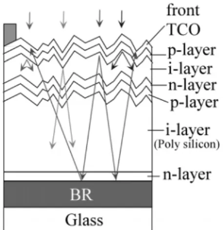
1
Fig. 1. Schematic ray diagram of light trapping in a tandem cell where front surface texture was achieved by surface roughness of polycrystalline silicon. An ideal situation where the unabsorbed long wavelength light remains confined to the active layer of the bottom cell. Here top four colored downward arrows in each of the subfigures signify color of broad band solar radiation, with purple, blue as short wavelengths and green, red as long wavelengths
Fig. 2. Schematic ray diagram of actual light path in a tandem In practice the ideal situation may not be achievable and the back reflected long wavelength light may travel through doped layers and to top cell as well. An attempt to achieve the ideal scheme is to use intermediate reflector21,35)
solar cell can be more than that of a single junction solar cell
under the broad band AM1.5G insolation
27). The primary advantage of a tandem solar cell is that light absorption is divided among two component cells, where top cell is made of a relatively wider band gap material so that high energy photons are absorbed in the top cell while relatively low energy photons are transmitted through it. This unabsorbed light then enters a relatively thicker second cell made up of lower band gap material. This technique of spectrum splitting is more popular in practical sense than other techniques where mirror or gratings-like optical elements are used to split the solar spectra that are then incident into separate cells
28-33).
2. Techniques adapted for light trapping
To the best of our knowledge, literature on effect of optical confinement in a tandem solar cell can be found as early as 1988
7), in which textured tin oxide front electrode and indium tin oxide/Ag back reflector (BR) was reported to provide light trapping in a silicon carbide (top cell active layer), silicon germanium (bottom cell active layer) tandem cell structure
7), leading to improved device performance. In 1997 fabrication of micro-morph solar cells were reported
6,8)while a similar investigation was reported four years later in 2001 by Schropp et al.
34). The difference in these two investigations are that the former inves- tigations
6,8)were based on back reflector coated glass superstrate,
while the later one
34)was of deposited tandem cell on stainless steel substrate. In these cells, light confinement was enhanced due to surface morphology of polycrystalline silicon layer.
Later micro-morph cells were fabricated with textured BR
15). Fig. 1 schematically demonstrates the ideal or expected ray diagram of trapped light in the bottom cell and Fig. 2 indicates that actual ray diagram in this configuration is different from the expected one. It is straight forward to be able to enhance current density of a tandem cell by light trapping.
It appears that the investigation of light trapping in tandem cell started with surface morphology of polycrystalline silicon layer. In principle, if the technique is designed and implemented properly whereby the light is confined within surface of the active layer (as demonstrated in Fig. 1), it can become one of the most effective methods in enhancing device performance. However, this does not happen in practice because trapped light travels to doped layers as well and also not all types of solar cells are made of polycrystalline silicon. Therefore, alternative methods are necessary to achieving surface texture and improvement in light trapping.
Several methods were proposed for surface texturing of the
transparent electrodes, glass superstrate etc so that cells that do
not have polycrystalline material can also have benefits of the
light trapping. Low pressure chemical vapor deposition (LPCVD)
is found to be promising in that respect. ZnO films deposited by
this LPCVD method shows highly textured surface useful for
the light trapping. Advantage of the technique is that the film
becomes self textured, and no chemical or physical method is
necessary for surface texturing. However it may be possible that
due to high level of surface texturing some localized surface defects can also be created that may degrade cell performance
36). Few other methods of texturing TCO are high deposition rate in a reactive mid-frequency sputter deposition of AZO
37), LP CVD deposited AZO may have better performance
38), excimer laser annealing and chemical etching of AZO
39)etc.
2.1 Textured front surface
Intrinsic hydrogenated amorphous silicon (a-Si:H), amorphous silicon germanium (a-SiGe:H) have reasonable optoelectronic properties to be used in tandem solar cell. The intrinsic a-Si:H have wider optical gap (1.7~1.8 eV) and hence good component for the top cell. Although a-Si/ a-Si tandem cell
19,40)can be fabricated but performance of the bottom cell will remain low, as a result lower tandem cell efficiency can be obtained (8.1%
19)).
A similar a-Si/a-Si tandem cell with textured SnO
2front (transparent conducting oxide or TCO) electrode was reported in 1989 having a relatively higher efficiency (9.3%
40)). It was observed that front surface texturing can reduce reflection loss of incident light
5,8); this is effective in a broader wavelength range as compared to anti reflection coating
41,42)where the later is wavelength dependant.
In order to enhance effect of front surface texturing, texturing of glass superstrate can be advantageous
43-46)over which ZnO can be deposited
47). Another approach is texturing the TCO front electrode. Several attempts in this direction showed its benefit, eg. a double layer of indium tin oxide (ITO) and aluminum doped zinc oxide (AZO) multi textured front electrode
20), transparent nano textured front electrode, low pressure chemical vapor deposition (LPCVD) grown boron doped zinc oxide (BZO)
48,49)to mention the few.
Depending on the surface texture, the front surface reflectivity can simply be expressed as
50)R = (R
flat)
n(1)
where R
flatis flat surface reflectivity and n is a number dependant on type of surface texture.
2.2 Back Reflector (BR)
The back reflector (is a special kind of mirror that) reflects the light back to the solar cell for further absorption. Depending on the type of mirror, that is flat or textured, the light trapping can be retro reflective or diffused reflective. Textured back reflector are preferable than a simple smooth BR
5,8,10). In a textured BR,
the reflected light remains diffused, thereby increasing average optical path length of reflected light within the cell and also raising a possibility of keeping more light outside the escape cone and thereby enhanced light trapping
10). A typical expected signature of light trapping is enhanced red response of external quantum efficiency (EQE) spectra. Various types of textured BR have been used so far, like the following: randomly textured glass
44)) or any other substrate
5,51,52), Si substrates
5,51,53,54)plastic substrate
52), photonic plasmonic crystal BR
55), varying surface texture of Ag/AZO BR
56), Ag nano particle used in the BR
57)for strong scattering of long wavelength light
58), surface textured electrically conductive photonic crystal back reflector
59), nano textured Ag BR
60), patterned BR
18), 3D photonic crystal intermediate reflector
61)) etc. At the front side of the solar cell, transparency and diffused transmission of the front electrode is another important necessity for light trapping
62).
3. Modeling, simulation, theory
Theoretical investigation shows that efficiency of a tandem cell can be improved by light trapping
9,10). There exists a tradeoff of light trapping among the two components of tandem cell
63). It is simple to understand that for a constant incident light (AM1.5G insolation) the light trapping and management can cause change in light absorption in the component cells. In other words, if more light is absorbed in the top cell then available light for the bottom cell becomes lower. This may result in a top cell short circuit current density (J
sc1) becoming larger than that of the bottom cell (J
sc2), or J
sc1> J
sc2. Then the output short circuit current density (J
sc) of a two terminal tandem cell becomes bottom cell limited, or J
sc= J
sc2. A reverse situation can arise when the bottom cell absorbs more light. In either of the cases, a light equivalent to the difference between the top and bottom cell current density ( ∆ J
sc12= J
sc1~ J
sc2) will be lost. Such a cell will perform poorer than its capability, primarily because of poorer light management. One simple rule that is followed in fabricating a tandem cell by all is, top cell is made thinner than the bottom cell. Although light trapping can raise the current density of all the tandem cells (irrespective of whether the cell structure is optimized or not), however, in order to fully utilize the capability of light trapping, an improved method of optimization becomes necessary.
Several attempts have been made in that direction. Simulation of light trapping using PC-1D
64), analysis of light trapping by ray tracing
5,51,65,66), are few of them.
The optically enhanced EQE (or EQE
2) can be expressed in
Fig. 3. Ideal division of solar spectra for top and bottom cell of a tandem solar cell. In reality, Si tandem solar cell does not follow this division and absorption edge of the materials are not sharp
Fig. 4. Typical external quantum efficiency (EQE) of a tandem solar cell under various stages of light trapping. 1-without light trapping, 2-with front surface texture, 3-with smooth BR, 4-with textured BR. The effects on the sequence 1-4 are additive, meaning 4-front texture + textured BR, 3- front texture + smooth BR, etc. The traces are for demonstration purpose
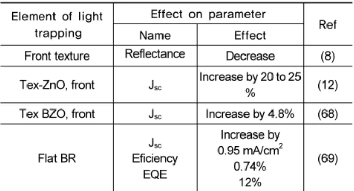
Table 1. Effect of light trapping on performance of a photo voltaic device
Element of light trapping
Effect on parameter Name Effect Ref
Front texture Reflectance Decrease (8)
Tex-ZnO, front Jsc Increase by 20 to 25
% (12)
Tex BZO, front Jsc Increase by 4.8% (68)
Flat BR Jsc
Eficiency EQE
Increase by 0.95 mA/cm2
0.74%
12%
(69)
terms of EQE without light trapping, EQE
1as follows
67):
EQE
2= EQE
1(1+x) (2)
Here x is wavelength dependant EQE enhancement factor
5,67). Similarly, the optically enhanced short circuit current density (J
sc2) can be expressed in terms of J
scwithout light trapping (J
sc1) as
J
sc2= J
sc1(1+y) (3)
y = q/(hc)∫(EQE
2-EQE
1) ( )d ,
here q charge of electron, h Plank’s constant, c speed of light,
is AM1.5 spectra, is wavelength.
Using a simple logic and ideal sharp band structure of materials, one can say that the usable part of solar spectra should be divided into two halves, where the shorter wavelength half should be allocated for the top cell and the bottom cell should be exposed by the second half of the spectra. Based on this, it can be suggested that the allocated spectral range for the top cell should be below 650 nm (Fig. 3) while that of the bottom cell should be 650 to 1200 nm, assuming 1200 nm is the usable long wavelength limit.
In summary, the effect of light trapping in a tandem solar cell can be described by EQE spectra, as given in Fig. 4. At the beginning, the quantum efficiency spectra of the cell will enhance due to successful light trapping, this will lead to enhanced current density and hence efficiency of the device.
Additional key components for improved device performances are, improved optoelectronic properties of the cell layers
70). Various works have been reported and also going on to improve material and hence further enhancement of device performance.
As this topic outside the scope of this article, so we prefer not to discuss it any further.
4. Conclusions
State of the art design of a two terminal tandem solar cell
should include opto-electronic aspects of the device in such a
way that high V
ocand J
scare achievable. High J
sccan only be
achieved when current generated by the top and bottom cells are
equal. In order to achieve high J
scan optimization is needed with
of thickness of all the layers of the device, texture of front and
back surfaces, and back reflector. Optimization of design of a
tandem solar cell is a complicated process, as it involves
optoelectronic properties of top and bottom cells. Under a
constant illumination a tradeoff in absorption among top and
bottom cell exists that depend on material and structural design of the layers of the component cells. In a tandem solar cell a higher open circuit voltage is achievable but J
scor current density decreases in comparison to that of a single junction solar cell. Effective light trapping can improve the current density of both the top and bottom cells and hence the overall device efficiency can be improved. Several different optimized cell structure is possible that may be unique to material and design of the cells, yet the fundamentals of all these is to incorporate textured front surface and back reflector for a state of the art tandem solar cell.
Acknowledgments
This work was supported by the New & Renewable Energy Core Technology Program of the Korea Institute of Energy Technology Evaluation and Planning (KETEP) granted financial resource from the Ministry of Trade, Industry & Energy, and Republic of Korea (No. 20133030010930).
This work was supported by the Human Resources Development program (No. 20144030200580) of the Korea Institute of Energy Technology Evaluation and Planning (KETEP) grant funded by the Korea government Ministry of Trade, Industry and Energy.
References
1. P. Campbell, “Light trapping in textured solar cells”, Sol Energy Mater, 21 (1990) 165-172.
2. E. Yablonovitch, G.D. Cody, “Intensity enhancement in tex- tured optical sheets for solar cells”, IEEE Trans. Electron Devices, ED-29 (1982) 300-305.
3. B.W. Faughnan, “Experimental observation of light trapping in hydrogenated amorphous silicon solar cells”, J Appl Phys, 58 (1985) 2746-2750.
4. P. Campbell, M.A. Green, “Light trapping properties of pyr- amidally textured surfaces”, J Appl Phys, 62 (1987) 243-249.
5. S.M. Iftiquar, J. Jung, C. Shin, H. Park, J. Park, J. Jung, J. Yi,
“Light management for enhanced efficiency of textured n-i-p type amorphous silicon solar cell”, Sol Energ Mater Sol Cells, 132 (2014) 348-355.
6. Y. Kenji, S. Takayuki, Y. Masashi, N. Akihiko, “Optical Confinement Effect for below 5 µ m Thin Film Poly-Si Solar Cell on Glass Substrate”, Jpn. J. Appl. Phys., 36 (1997) L569.
7. D.E. Carlson, R.R. Arya, M.S. Bennett, A. Catalano, R.C.
D'Aiello, C.R. Dickson, C.M. Fortmann, B. Goldstein, J.
Morris, J.L. Newton, S. Wiedeman, “Progress toward high ef- ficiency multijunction cells and submodules at Solarex”, Solar Cells, 24 (1988) 165-169.
8. A. Nakajima, T. Suzuki, M. Yoshimi, K. Yamamoto,
“Enhancement of optical absorption for below 5 μm thin-film poly-Si solar cell on glass substrate”, Sol Energ Mater Sol Cells, 48 (1997) 287-294.
9. J. Müller, B. Rech, J. Springer, M. Vanecek, “TCO and light trapping in silicon thin film solar cells”, Sol. Energy, 77 (2004) 917-930.
10. A.V. Shah, M. Vaněček, J. Meier, F. Meillaud, J. Guillet, D.
Fischer, C. Droz, X. Niquille, S. Faÿ, E. Vallat-Sauvain, V.
Terrazzoni-Daudrix, J. Bailat, “Basic efficiency limits, recent experimental results and novel light-trapping schemes in a-Si:H, μc-Si:H and 'micromorph tandem' solar cells”, J Non Cryst Solids, 338-340 (2004) 639-645.
11. J. Krc, K. Brecl, F. Smole, M. Topic, “The effects of enhanced light trapping in tandem micromorph silicon solar cells”, Sol Energ Mater Sol Cells, 90 (2006) 3339-3344.
12. P. Kumar, M. Kupich, W. Bock, R.O. Dusane, B. Schroeder,
“Microcrystalline single and double junction silicon based solar cells entirely prepared by HWCVD on textured zinc oxide sub- strate”, J Non Cryst Solids, 352 (2006) 1855-1858.
13. A. Bielawny, J. Üpping, P.T. Miclea, R.B. Wehrspohn, C.
Rockstuhl, F. Lederer, M. Peters, L. Steidl, R. Zentel, S.M.
Lee, M. Knez, A. Lambertz, R. Carius, “3D photonic crystal in- termediate reflector for micromorph thin-film tandem solar cell”, Phys. Status Solidi A Appl. Mater. Sci., 205 (2008) 2796-2810.
14. K. Bittkau, T. Beckers, “Near-field study of light scattering at rough interfaces of a-Si:H/μc-Si:H tandem solar cells”, Phys.
Status Solidi A Appl. Mater. Sci., 207 (2010) 661-666.
15. J.S. Cho, S. Baek, K.H. Yoon, “Enhancement of light trapping by textured back electrodes in tandem micromorph n-i-p silicon thin film solar cells”, Curr. Appl. Phys., 11 (2011) S2-S7.
16. A. Feltrin, T. Meguro, M. Ichikawa, F. Sezaki, K. Yamamoto,
“Light scattering and parasitic absorption in thin film silicon so- lar cells containing metal nano particles”, J. Photonics Energy, 1 (2011) 017003.
17. K.C. Lai, F.J. Tsai, J.H. Wang, C.H. Yeh, M.P. Houng,
“Texturing of the back reflector for light trapping enhancement in micromorph thin film solar cells”, Thin Solid Films, 519 (2011) 3946-3949.
18. H. Sai, M. Kondo, “Light trapping effect of patterned back sur- face reflectors in substrate-type single and tandem junction thin-film silicon solar cells”, Sol Energ Mater Sol Cells, 95 (2011) 131-133.
19. K. Söderström, J. Escarré, O. Cubero, F.J. Haug, S. Perregaux, C. Ballif, “UV-nano-imprint lithography technique for the rep- lication of back reflectors for n-i-p thin film silicon solar cells”, Prog Photovoltaics Res Appl, 19 (2011) 202-210.
20. M. Boccard, P. Cuony, C. Battaglia, S. Hänni, S. Nicolay, L.
Ding, M. Benkhaira, G. Bugnon, A. Billet, M. Charrière, K.
Söderström, J. Escarré, F. Sculati-Meillaud, M. Despeisse, C.
Ballif, “Nanometer- and micrometer-scale texturing for high-ef- ficiency micromorph thin-film silicon solar cells”, IEEE J.
Photovoltaics, 2 (2012) 83-87.
21. T. Meguro, A. Feltrin, T. Suezaki, M. Ichikawa, T.
Kuchiyama, D. Adachi, O. Inaki, K. Yoshikawa, G. Koizumi, H. Uzu, H. Ueda, T. Uto, T. Fujimoto, T. Irie, H. Hayakawa, N. Nakanishi, M. Yoshimi, K. Yamamoto, “Advanced light trapping of high-efficiency thin film silicon solar cells”, Jpn. J.
Appl. Phys., 51 (2012) 10nb02.
22. S.M. Iftiquar, J.C. Lee, J. Lee, Y. Kim, J. Jang, Y.J. Lee, J. Yi,
“Light management and efficient carrier generation with a highly transparent window layer for a multijunction amor- phous silicon solar cell”, J. Photonics Energy, 3 (2013) 033098.
23. S.M. Iftiquar, J.C. Lee, J. Lee, J. Jang, Y.-J. Lee, J. Yi, “Single- and Multiple-Junction p-i-n Type Amorphous Silicon Solar Cells with p-a-Si1-xCx:H and nc-Si:H Films”, in: I. Yun (Ed.) Photodiodes - from fundamentals to applications Intech, Croatia, 2012, pp. 289-311.
24. R.E.I. Schropp, H. Li, R.H. Franken, J.K. Rath, C.H.M. van der Werf, J.W.A. Schüttauf, R.L. Stolk, “Nanostructured thin films for multiband-gap silicon triple junction solar cells”, Thin Solid Films, 516 (2008) 6818-6823.
25. G. Yue, L. Sivec, J.M. Owens, B. Yan, J. Yang, S. Guha,
“Optimization of back reflector for high efficiency hydro- genated nanocrystalline silicon solar cells”, Appl Phys Lett, 95 (2009) 263501.
26. D.J. You, S.H. Kim, H. Lee, J.W. Chung, S.T. Hwang, Y.H.
Heo, S. Lee, H.M. Lee, “Recent progress of high efficiency Si thin-film solar cells in large area”, Prog Photovoltaics Res Appl, 23 (2015) 973-988.
27. S.M. Iftiquar, J. Park, C. Shin, J. Jung, S. Bong, V.A. Dao, J.
Yi, “Present Status and Prospects of Thin Film Silicon Solar Cells”, Current Photovoltaic Research, 2 (2014) 41-47.
28. A. Bielawny, P.T. Miclea, A.V. Rhein, R.B. Wehrspohn, S.
Van Riesen, S. Glunz, “Dispersive elements for spectrum split- ting in solar cell applications”, in: Photonics for Solar Energy Systems, Strasbourg, 2006.
29. A. Goetzberger, J.C. Goldschmidt, M. Peters, P. Löper, “Light trapping, a new approach to spectrum splitting”, Sol Energ Mater Sol Cells, 92 (2008) 1570-1578.
30. J.D. McCambridge, M.A. Steiner, B.L. Unger, K.A. Emery, E.L. Christensen, M.W. Wanlass, A.L. Gray, L. Takacs, R.
Buelow, T.A. McCollum, J.W. Ashmead, G.R. Schmidt, A.W.
Haas, J.R. Wilcox, J. Van Meter, J.L. Gray, D.T. Moore, A.M.
Barnett, R.J. Schwartz, “Compact spectrum splitting photo- voltaic module with high efficiency”, Prog Photovoltaics Res Appl, 19 (2011) 352-360.
31. X. Wang, N. Waite, P. Murcia, K. Emery, M. Steiner, F.
Kiamilev, K. Goossen, C. Honsberg, A. Barnett, “Lateral spec- trum splitting concentrator photovoltaics: Direct measurement of component and submodule efficiency”, Prog Photovoltaics Res Appl, 20 (2012) 149-165.
32. J.M. Russo, D. Zhang, M. Gordon, S. Vorndran, Y. Wu, R.K.
Kostuk, “Spectrum splitting metrics and effect of filter charac- teristics on photovoltaic system performance”, Opt. Express,
22 (2014) A528-A541.
33. Y. Yao, H. Liu, W. Wu, “Spectrum splitting using multi-layer dielectric meta-surfaces for efficient solar energy harvesting”, Appl Phys A, 115 (2014) 713-719.
34. R.E.I. Schropp, C.H.M. Van Der Werf, M.K. Van Veen, P.A.T.T. Van Veenendaal, R. Jimenez Zambrano, Z. Hartman, J. Löffler, J.K. Rath, “Thin film a-Si/poly-Si multibandgap tan- dem solar cells with both absorber layers deposited by Hot Wire CVD”, in: M. Stutzmann, J. Boyce, J.D. Cohen, R. Collins, J.
Hanna (Eds.) Amorphous and Heterogeneous Silicon Based Films 2001, San Francisco, CA, 2001, pp. A1561-A1566.
35. A. Feltrin, T. Meguro, E. Van Assche, T. Suezaki, M. Ichikawa, T. Kuchiyama, D. Adachi, O. Inaki, K. Yoshikawa, G. Koizumi, H. Uzu, H. Ueda, T. Uto, T. Fujimoto, T. Irie, H. Hayakawa, N. Nakanishi, M. Yoshimi, K. Yamamoto, “Advanced light trapping designs for high efficiency thin film silicon solar cells”, Sol Energ Mater Sol Cells, 119 (2013) 219-227.
36. J. Yin, H. Zhu, Y. Wang, Z. Wang, J. Gao, Y. Mai, Y. Ma, M.
Wan, Y. Huang, “A study of ZnO:B films for thin film silicon solar cells”, Appl Surf Sci, 259 (2012) 758-763.
37. S. Calnan, J. Hüpkes, B. Rech, H. Siekmann, A.N. Tiwari,
“High deposition rate aluminium-doped zinc oxide films with highly efficient light trapping for silicon thin film solar cells”, Thin Solid Films, 516 (2008) 1242-1248.
38. A. Čampa, M. Meier, M. Boccard, L.V. Mercaldo, M. Ghosh, C. Zhang, T. Merdzhanova, J. Krč, F.J. Haug, M. Topič,
“Micromorph silicon solar cell optical performance: Influence of intermediate reflector and front electrode surface texture”, Sol Energ Mater Sol Cells, 130 (2014) 401-409.
39. C. Charpentier, R. Boukhicha, P. Prod'Homme, T. Emeraud, J.F. Lerat, P.R.I. Cabarrocas, E.V. Johnson, “Evolution in morphological, optical, and electronic properties of ZnO:Al thin films undergoing a laser annealing and etching process”, Sol Energ Mater Sol Cells, 125 (2014) 223-232.
40. K. Asaoka, M. Yamaguchi, H. Yamagishi, W.A. Nevin, H.
Nishio, T. Endoh, K. Tsuge, Y. Tawada, “Light-induced ef- fects in a-Si/a-Si two-stacked tandem junction solar cells”, J Non Cryst Solids, 115 (1989) 24-26.
41. R. Brendel, A. Gier, M. Mennig, H. Schmidt, J.H. Werner,
“Sol-gel coatings for light trapping in crystalline thin film sili- con solar cells”, J Non Cryst Solids, 218 (1997) 391-394.
42. K. Ryu, Y.J. Lee, M. Ju, H. Choi, B. Kim, J. Lee, W. Oh, K.
Choi, N. Balaji, J. Yi, “Optimal indium tin oxide layer as anti reflection coating for crystalline silicon solar cell with shallow emitter”, Thin Solid Films, 521 (2012) 50-53.
43. T. Doege, M. Neander, U. Blieske, A. Prat, P. Gayout,
“Textured glass increases light transmission in solar modules”, Glass Res., 12 (2002) 5-7.
44. E. Bunte, W. Zhang, J. Hüpkes, “Preparation and topography analysis of randomly textured glass substrates”, J. Vac. Sci.
Technol. A Vac. Surf. Films, 28 (2010) 1255-1258.
45. S. Neubert, S. Ring, F. Welker, S. Götzendörfer, F. Ruske, B.
Stannowski, R. Schlatmann, B. Rech, “Very thin, highly-con-
ductive ZnO: Al front electrode on textured glass as substrate for thin-film silicon solar cells”, Physica Status Solidi Rapid Res. Lett., 8 (2014) 44-47.
46. W. Zhang, U.W. Paetzold, M. Meier, A. Gordijn, J. Hüpkes, T. Merdzhanova, “Thin-film silicon solar cells on dry etched textured glass”, in: Energy Procedia, 2014, pp. 151-159.
47. J. Steinhauser, J.F. Boucher, E. Omnes, D. Borrello, E.
Vallat-Sauvain, G. Monteduro, M. Marmelo, J.B. Orhan, B.
Wolf, J. Bailat, S. Benagli, J. Meier, U. Kroll, “Improving low pressure chemical vapor deposited zinc oxide contacts for thin film silicon solar cells by using rough glass substrates”, Thin Solid Films, 520 (2011) 1218-1222.
48. Y. Abe, T. Kagei, P. Sichanugrist, M. Konagai, “Development of double-textured ZnO:B substrates for improving micro- crystalline silicon solar cell performance”, IEEE J. Photovoltaics, 4 (2014) 1374-1379.
49. M.L. Addonizio, L. Fusco, “Preparation method of dou- ble-textured ZnO:B films deposited by MOCVD on plasma etched polymer buffer”, J Alloys Compd, 622 (2015) 851-858.
50. S.M. Iftiquar, J. Jung, H. Park, J. Cho, C. Shin, J. Park, J. Jung, S. Bong, S. Kim, J. Yi, “Effect of light trapping in an amor- phous silicon solar cell”, Thin Solid Films, 587 (2015) 117–125.
51. S.M. Iftiquar, J. Jang, H. Park, C. Shin, J. Park, J. Jung, S. Kim, J. Yi, “Analysis of optical absorption and quantum efficiency due to light trapping in a n-i-p type amorphous silicon solar cell with textured back reflector”, Phys. Status Solidi A Appl.
Mater. Sci., 211 (2014) 924-931.
52. P. Alpuim, A. Samantilleke, E. Marins, F. Oliveira, M.F.
Cerqueira, L. Rebouta, S. Stefanov, S. Chiussi, C. Serra, J.E.
Bourée, “Amorphous silicon thin-film solar cells deposited on flexible substrates using different zinc oxide layers”, 23rd International Conference on Amorphous and Nanocrystalline Semiconductors, ICANS23, 7 (2010) 1061-1064.
53. H. Angermann, J. Rappich, C. Klimm, “Wet-chemical treat- ment and electronic interface properties of silicon solar cell sub- strates”, Cent. Eur. J. Phys., 7 (2009) 363-370.
54. M. Asad, M. Kowsari, M.H. Sheikhi, “Enhancement of nano-/
microtextured crystalline silicon solar cells efficiency using hy- drogen plasma surface treatment”, Optik, 126 (2015) 5762-5766.
55. R. Biswas, S. Pattnaik, C. Xu, J. Bhattacharya, N. Chakravarty, V. Dalal, “Enhancement of solar cells with photonic and plas- monic crystals - Overcoming the Lambertian limit”, J Mater Res, 28 (2013) 1021-1030.
56. W. Böttler, V. Smirnov, J. Hüpkes, F. Finger, “Variation of back reflector morphology in n-i-p microcrystalline silicon thin film solar cells using texture-etched ZnO”, J Non Cryst Solids, 358 (2012) 2474-2477.
57. J. Chantana, Y. Yang, Y. Sobajima, C. Sada, A. Matsuda, H.
Okamoto, “Localized surface plasmon enhanced microcrystal- line-silicon solar cells”, J Non Cryst Solids, 358 (2012) 2319-2323.
58. S. Kim, J. Lee, V.A. Dao, S. Ahn, S.Q. Hussain, J. Park, J.
Jung, C. Lee, B.S. Song, B. Choi, Y.J. Lee, S.M. Iftiquar, J. Yi,
“Investigation of electrical and optical properties of highly
transparent TCO/Ag/TCO multilayer”, J. Nanosci. Nanotechnol., 15 (2015) 2247-2252.
59. P. Chen, G. Hou, Q. Fan, Q. Huang, J. Zhao, J. Zhang, J. Ni, X. Zhang, Y. Zhao, “An efficient light trapping scheme based on textured conductive photonic crystal back reflector for per- formance improvement of amorphous silicon solar cells”, Appl Phys Lett, 105 (2014) 073506.
60. J.S. Cho, S. Baek, S.H. Park, J.H. Park, J. Yoo, K.H. Yoon,
“Effect of nanotextured back reflectors on light trapping in flexi- ble silicon thin-film solar cells”, Sol Energ Mater Sol Cells, 102 (2012) 50-57.
61. J. Üpping, A. Bielawny, R.B. Wehrspohn, T. Beckers, R.
Carius, U. Rau, S. Fahr, C. Rockstuhl, F. Lederer, M. Kroll, T.
Pertsch, L. Steidl, R. Zentel, “Three-dimensional photonic crystal intermediate reflectors for enhanced light-trapping in tandem solar cells”, Adv Mater, 23 (2011) 3896-3900.
62. M. Berginski, J. Hüpkes, W. Reetz, B. Rech, M. Wuttig,
“Recent development on surface-textured ZnO:Al films pre- pared by sputtering for thin-film solar cell application”, Thin Solid Films, 516 (2008) 5836-5841.
63. L. Bai, B. Liu, J. Fan, D. Zhang, C. Wei, J. Sun, Y. Zhao, X.
Zhang, “The trade-off of light trapping between top and bottom cell in micromorph tandem solar cells with sputtering ZnO:Al glass substrate”, J Power Sources, 266 (2014) 138-144.
64. P.A. Basore, “Numerical Modeling of Textured Silicon Solar Cells Using PC-1D”, IEEE Trans. Electron Devices, 37 (1990) 337-343.
65. S.J. Byun, S.Y. Byun, J. Lee, J.W. Kim, T.S. Lee, K. Cho, D.
Sheen, S.J. Tark, D. Kim, W.M. Kim, “Analysis of light trap- ping effects in Si solar cells with a textured surface by ray tracing simulation”, Curr. Appl. Phys., 11 (2011) S23-S25.
66. S.Y. Byun, S.J. Byun, J.K. Lee, J.W. Kim, T.S. Lee, D. Sheen, K. Cho, S.J. Tark, D. Kim, W.M. Kim, “An efficient ray trac- ing algorithm for the simulation of light trapping effects in Si so- lar cells with textured surfaces”, J. Nanosci. Nanotechnol., 12 (2012) 3224-3227.
67. H. Park, S.M. Iftiquar, H.W. Kim, J. Lee, A.H.T. Le, J. Yi,
“Diffused transmission and texture-induced defect with trans- parent conducting oxide front electrode of amorphous silicon solar cell”, Semicond Sci Technol, 28 (2013) 115012.
68. B. Janthong, T. Krajangsang, A. Hongsingthong, L. Zhang, P.
Sichanugrist, M. Konagai, “Improvement of internal light-trap- ping for silicon based solar cells with a newly developed struc- ture”, in: 37th IEEE Photovoltaic Specialists Conference, PVSC 2011, Seattle, WA, 2011, pp. 000622-000625.
69. C. Ulbrich, A. Gerber, K. Hermans, A. Lambertz, U. Rau,
“Analysis of short circuit current gains by an anti-reflective tex- tured cover on silicon thin film solar cells”, Prog Photovoltaics Res Appl, 21 (2013) 1672-1681.
70. M. Fecioru-Morariu, B. Mereu, S. Bakehe, J. Kalas, O. Kluth, T. Eisenhammer, “High quality amorphous Si solar cells for large area mass production Micromorph tandem cells”, J Non Cryst Solids, 358 (2012) 2264-2267.