수치해석을 이용한 임베딩 패키지 솔더 조인트의 신뢰성에 미치는 에이징 효과 연구
조승현1·장준영2,3·고영배3,†
1동양미래대학교 기계공학과
2인하대학교 기계공학과
3한국생산기술연구원 금형기술그룹팀
Study on Effects of Solder Joint aging on the Reliability of Embedded Package Solder Joints using Numerical analysis
Seunghyun Cho1, Junyoung Jang2,3, and Youngbae Ko3,†
1Department of Mechanical Engineering, Dongyang Mirae University, 445, Gyeongin-ro, Guro-gu, Seoul 08221, Korea
2Department of Mechanical Engineering, Inha University, 100 Inha-ro, Nam-gu Incheon 22212, Korea
3Molds & Dies Technology R&D Group, KITECH, 156, Gaetbeol-ro, Yeonsu-gu, Incheon 21999, Korea (Received November 29, 2017: Corrected January 20, 2018: Accepted March 15, 2018)
초 록: 본 논문에서는 임베딩 패키지의 솔더 조인트 신뢰성에 미치는 솔더 조인트의 에이징 효과를 유한요소법에 의한 수치해석을 통해 연구하였다. SAC305 솔더 조인트의 에이징 시간은 0, 60, 180 일이 적용되었고 신뢰성 분석을 위해 패키 지 휨, ECS(Equivalent Creep Strain) 및 TSED(Total Strain Energy Density)이 분석되었다. 연구결과에 따르면 임베딩 패 키지의 휨이 비임베딩 패키지에 비해 감소하여 임베딩 패키지내 솔더 접합부의 신뢰성이 높을 것으로 예측되었다. 또한, 에이징 시간이 길수록 임베디드 패키지의 휨이 감소하지만 솔더 조인트의 신뢰성 수명도 감소할 것으로 분석되었다.
Abstract: In this paper, the effects of solder joint aging on the reliability of embedded package solder joints were investigated using numerical analysis by finite element method. Solder joints were SAC305 with aging time 0, 60, 180 days. For reliability analysis, warpage of package and equivalent creep strain (ECS) and total strain energy density (TSED) of solder joint were analyzed. The analysis results show that the package warpage is decreased in the case of the embedded package compared to the non embedded package, and the reliability life of the solder joint is predicted to be high. Also, it was interpreted that the longer the aging time, the less the warpage of the embedded package, but the reliability life of the solder joint would be shortened.
Keywords: Embedded package, SAC305, ANAND model, Warpage, TSED, FEM
1. 서 론
웨이퍼 레벨 패키지 (wafer level package, WLP)는 소형 칩 사이즈와 작은 핀 수를 구현할 수 있어 이미지센서, 전 력 관리 장치, 아날로그 장치 등에 적용되고 있다.1) WLP 신뢰성에 대한 연구는 주로 솔더 조인트(solder joint)를 대상으로 이루어지고 있는데 열적 피로(thermal fatigue) 는 신뢰성에 영향을 미치는 가장 큰 인자이다.2-5)유한요 소법을 이용한 수치해석으로 솔더 조인트의 신뢰성 연구 로써 Anand 등은 SAC 솔더 조인트를 점소성 구성 방정 식(viscoplastic constitutive equation)을 사용한 ANAND 모
델을 제시하여 고온에서 열거동 특성을 연구하였고,6) 이 후 ANAND 모델을 이용한 SAC 솔더 조인트의 크리프 거동과 신뢰성 연구가 활발하게 진행되었다.7-12)
전기 및 열적 저항을 낮춤으로써 I/O 밀도를 증가시키 고 복합 칩을 실장시킬 수 있는 장점으로 임베딩 기술을 WLP에 접목한 임베딩 웨이퍼 레벨 패키징(Embedded wafer level packaging, EMWLP)이 개발되면서 인쇄회 로기판(PCB)내부에 실장되는 칩(chip)이 패키지, 특히 솔 더 조인트의 신뢰성에 미치는 연구가 꾸준히 진행되고 있
다.13-18) 본 논문에서는 SAC솔더 조인트의 에이징(aging)에
따른 패키지 레벨의 휨(warpage), 솔더 조인트의 TECS(Total
†
Corresponding author E-mail: [email protected]
© 2018, The Korean Microelectronics and Packaging Society
This is an Open-Access article distributed under the terms of the Creative Commons Attribution Non-Commercial License(http://creativecommons.org/
licenses/by-nc/3.0) which permits unrestricted non-commercial use, distribution, and reproduction in any medium, provided the original work is
properly cited.
equivalent creep strain)와 TSED(Total strain energy density) 등을 분석함으로써 EMWLP에 적용된 SAC 솔더 조인트 의 열적 거동특성을 고찰하고 솔더 조인트의 신뢰성에 미 치는 에이징 효과를 분석하였다.
2. 해석 방법
2.1. 유한요소 모델링
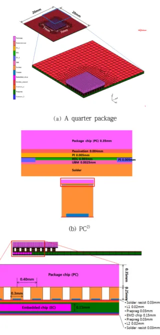
Fig. 1(a)~(c)는 임베딩 패키지의 유한요소 모델링을 보 여주는 그림들이다. 패키지는 Fig. 1(a)와 같이 1/4 형상만 을 8-노드를 갖는 육면체 메쉬를 사용하여 모델링하였고 PCB와 패키지 칩(package chip, PC)의 크기는 각각 20 mm× 20mm와 7 mm × 7 mm이다. Fig. 1(b)는 PC의 구
조로써 참고문헌2)의 구조를 인용하여 상세하게 모델링하 였다. Fig. 1(c)는 패키지의 단면을 나타낸 그림으로 솔더 조인트는 0.3 mm지름과 0.25 mm의 높이를 갖는 0.4 mm 피치의 원통형으로 모델링하였다. PCB는 2층 회로를 갖 고 상, 하 회로층의 잔동률은 각각 60%와 45%로 가정하 였으며 혼합 룰(Rule of mixture)을 적용하여 회로층을 모 델링하였다. 임베딩 칩(embedded chip, EC)의 두께는 0.15 mm이다. Table 1은 유한요소 모델링에 사용된 임베 딩 패키지의 재료 특성값이다.
2.2. 솔더 조인트의 ANAND 모델
솔더 조인트의 재료특성에 관한 ANAND 모델은 2가 지 특징을 가지고 있다.13) 첫째, ANAND 모델에는 명확 한 항복조건과 로딩/언로딩 기준이 없다. 또한 재료의 순 간적 반응은 현재 상태에 따라 달라지며 소성 변형률은 모든 응력 값에서 발생한다고 가정하였다. 둘째, 변형 저 항이라고 하는 내부 변수 “s”는 등가 응력에 비례한다.
ANAND 모델을 위한 유동 방정식과 전개 방정식은 다음 과 같다.
유동 방정식 :
(1)
전개 방정식 :
(2)
(3)
(4)
위 방정식은 A, Q, ξ, m, h0, , n, a, s0 is 9개 재료 파라 메타를 갖는데 여기서 s0는 변형 저항의 변화를 결정하는
dεp
---dt A ξσ ---s
⎝ ⎠⎛ ⎞ sinh
m1
---- Q
kT---
⎝– ⎠
⎛ ⎞ exp
=
ds
dt--- h0BaB --- dεB p
---dt
=
B 1 s s* –----
=
s* sˆ 1 A--- dεp
---dt Q kT---
⎝ ⎠⎛ ⎞ exp
n
=
sˆ Table 1. Material properties of package19)
Materials Elastic modulus,
GPa CTE, ppm/oC Poission’s ratio
Package chip, PC 130 2.6 0.28
Passivation 105 11 0.24
UBM 50 16 0.35
RDL 130 16.8 0.34
Polyimide 1.2 52 0.34
Copper 130 16.8 0.34
Solder 50 24.5 0.35
Circuit layer 1 79 30 0.324
Prepreg 25 15 0.3
Embedded chip, EC 130 2.6 0.28
Circuit layer 2 60 35 0.318
Fig. 1. FEA model of embedded package.
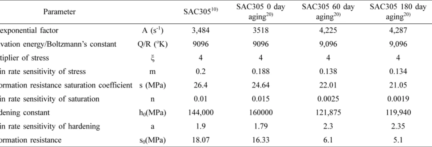
데 필요한 변형 저항의 초기 값을 나타낸다. SAC305 솔 더의 크리프 해석을 위해 본 논문에서는 Table 2와 같이 100oC에서 에이징한 4종의 솔더에 대한 ANAND 파라메 타 값을 사용하였다.
2.3. 해석 조건
임베딩 패키지의 솔더에 미치는 임베딩 칩의 영향을 분
석하기 위해서 Fig. 2와 같이 임베딩 칩이 없는 경우와 있 는 경우에 대해 해석을 수행하였다. 임베딩 칩의 사이즈 는 3 mm × 3 mm × 0.15 mm이고 패키징의 중심에 위치하 도록 하였다. Fig. 3은 해석에 적용된 TC조건을 보여주고 있다. 일반적으로 솔더는 실장 후 리플로우 과정에서 잔 류응력이 발생하기 때문에 초기 잔류응력이 크리프 변형 특성에 영향을 미치지만 잔류응력을 정량적으로 평가하 기가 어렵고, TC 조건의 영향을 분석한다는 측면에서 본 논문에서는 25oC에서 잔류응력이 없다고 가정하였다. 해 석에 사용된 TC조건은 25oC에서 125oC로 50oC/분 속도 로 온도가 상승한 후 10분간 유지하였고, 이후 동일한 속 도로 -40oC까지 감온되어 10분간 유지된 후 다시 25oC로 상승하는 사이클을 10회 반복하도록 하였다.
3. 결과 및 고찰
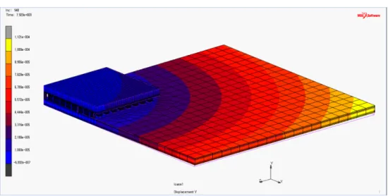
Fig. 4는 솔더 조인트의 재료가 180일 에이징된 SAC305 일 때 임베딩 패키지에서 발생한 휨 분포를 보여주고 있 다. 휨의 분포는 TC 10회 사이클의 125oC인 Fig. 3의 ① 위치에서 관찰한 결과로써 패키지 칩이 있는 방향으로 오 목한 형태로 발생하였고 휨의 형태는 솔더 조인트의 종 류와는 상관없이 모두 오목한 형태이다. 패키지의 휨은 패키지의 구성요소인 칩, 솔더, PCB 등 이종재료간 열팽 창차이로 발생하는데, 패키징의 휨은 PCB 휨의 영향이 가장 크다. 이것은 PCB를 구성하고 있는 재료간 열팽창 량 차이가 크고, PCB의 사이즈가 커서 패키지의 중심에 서 외곽으로 갈수록 PCB 휨이 크게 발생하기 때문이다.
Fig. 5(a)는 솔더 조인트 재료에 따라 임베딩 패키지에 서 발생한 휨을 TC시간의 함수로 나타낸 결과이다. 임베 딩 패키지의 휨은 TC 조건에 따라 발생하였는데, 온도가 125oC일 때 임베딩 칩이 인쇄회로기판 내부에 실장되지 않은 패키지에서 최대 휨이 발생하였다. 그러나 -40oC 온 도에서는 임베딩 패키지가 에이징하지 않은 솔더 조인트 를 사용했을 때 최대 휨이 발생하였다. Fig. 5(b)는 TC 10 회에서 발생한 (+)방향 휨과 (-)방향 휨의 최대 차이를 솔 더 조인트 재료에 따라 나타낸 결과이다. 즉, Fig. 3의 온 Table 2. Parameters of ANAND model for solder materials
Parameter SAC30510) SAC305 0 day
aging20)
SAC305 60 day aging20)
SAC305 180 day aging20)
Pre-exponential factor A (s-1) 3,484 3518 4,225 4,287
Activation energy/Boltzmann’s constant Q/R (oK) 9096 9096 9,096 9,096
Multiplier of stress ξ 4 4 4 4
Strain rate sensitivity of stress m 0.2 0.188 0.138 0.134
Deformation resistance saturation coefficient s (MPa) 26.4 24.64 22.01 21.05
Strain rate sensitivity of saturation n 0.01 0.015 0.0025 0.0019
Hardening constant h0(MPa) 144,000 160000 121,875 119,940
Strain rate sensitivity of hardening a 1.9 1.79 2.3 2.35
Deformation resistance s0(MPa) 18.07 16.33 6.1 5.1
Fig. 2. Parameter design (without & with EC) condition to analyze EC effect on embedded package warpage.
Fig. 3. Temperature profile for analysis of embedded package.
도 ①에서 발생한 휨과 온도 ②에서 발생한 휨의 차이이 다. 결과에 따르면 180일 에이징한 솔더 조인트가 적용된 임베딩 패키지의 휨이 가장 작게 발생하였고, 에이징하 지 않은 솔더 조인트가 적용될 때 가장 큰 휨이 발생하였 다. Fig. 5(a), (b)의 결과로부터 SAC305 솔더의 에이징 시 간이 증가할수록 임베딩 패키지의 휨이 감소하였다. 솔 더는 에이징 시간이 증가할수록 전단강도가 감소하는데 이러한 특성이 열변형량이 작은 칩과 큰 PCB사이의 변 형을 완충시키는 역할을 하여 패키지 휨이 감소하는 것
으로 판단된다.
Fig. 6은 에이징하지 않은 SAC305 솔더 조인트에서 발 생한 등가 크리프 변형률의 분포 결과로써 최대 등가 크 리프 변형률는 그림에서 표시한 바와 같이 최 외곽에서 발생하고 있다. 이것은 임베딩 패키지가 TC 조건에서 열 변형을 일으킬 때 최외곽 솔더 조인트에서 가장 큰 변형 에 대한 저항이 발생하기 때문이다. Fig. 7은 TC조건에서 Fig. 6에서 표시한 최 외곽 솔더 조인트에서 발생한 등가 크리프 변형률을 나타낸 결과이다. 등가 크리프 변형률 Fig. 4. Warpage distribution of embedded package with SAC305 solder joints after 180 days aging.
Fig. 5. Warpage of embedded package as material of solder joints.
Fig. 6. ECS distribution on solder joints of SAC305 with no aging.
Fig. 7. ECS of solder joints under thermal cycles conditions.
은 TC이 증가할수록 솔더 조인트에 누적되어 증가하였 다. 에이징을 하지 않은 솔더 조인트에서 최소 등가 크리 프 변형률이 발생하였고, 에이징 시간이 증가할수록 등 가 크리프 변형률은 증가하였다. 또한 임베딩 패키지의 경우가 일반 패키지에 비해 크리프 변형률이 작게 발생 하였다. 이와 같은 결과는 SAC305 솔더는 에이징 시간이 증가할수록 2차 크리프율이 증가하는 것으로 알려져 있 고13), 에이징 시간이 증가할수록 Table 2와 같이 솔더 조 인트의 변형 저항이 작아지기 때문에 크리프 변형률이 증 가하는 것으로 판단된다.
Fig. 8은 임베딩 패키지의 솔더 조인트에서 발생한 토 탈 변형에너지 밀도를 TC조건에 따라 나타낸 결과이다.
에이징이 되지 않은 솔더 조인트의 경우 각 TC 사이클당 변형에너지 밀도의 변동폭이 가장 크게 발생하였다. 또 한 TC 사이클이 증가할수록 증가율이 크지 않아서 TC 사이클 초기에는 가장 큰 변형에너지 밀도가 발생하였지 만 8회 사이클 이후에는 가장 낮은 변형에너지 밀도가 발 생하였다. 즉, 에이징 시간이 증가할수록 TC에 따라 발 생하는 변형에너지 밀도가 크게 증가하였다. 한편, 임베 딩 패키지의 솔더 조인트와 일반 패키지의 솔더 조인트 에서 발생한 변형에너지를 비교하면 임베딩 패키지의 솔 더 조인트에서 크게 발생하였다.
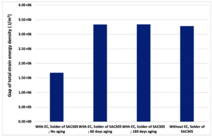
Fig. 9는 TC 10회때 임베딩 패키지의 솔더 조인트에서 발생한 토탈 변형률에너지 밀도의 변화폭을 나타낸 결과 이다. 에이징이 되지 않은 솔더 조인트에서 발생한 변형 에너지 밀도 폭이 가장 작게 발생하였고 에이징 시간이 증가할수록 변형에너지 밀도 폭이 크게 증가하였다. 일 반적으로 변형에너지 밀도가 증가하면 수명이 단축되기 때문에 Fig. 8과 Fig. 9의 결과로부터 에이징을 하면 솔더 조인트의 신뢰성 수명이 단축되지만 에이징 기간이 60일 이상이 되면 솔더 조인트의 신뢰성 수명에는 큰 영향이 없을 것으로 예측되었다. 또한 에이징 기간이 60일 이상 이 되면 임베딩 패키지와 일반 패키지에 적용된 솔더 조 인트의 신뢰성 수명도 유사할 것으로 예측되었다.
4. 결 론
본 논문에서는 임베딩 패키지 솔더 조인트의 신뢰성에 미치는 솔더 조인트의 에이징 효과를 유한요소법에 의한 수치해석으로 연구를 수행하였다. 해석 결과에 의하면 임 베딩 패키지의 경우가 일반 패키지에 비해 패키지의 휨 은 감소하였고, 솔더 조인트의 변형에너지 밀도가 증가 하여 신뢰성 수명이 낮을 것으로 예측되었다. 또한 솔더 조인트는 에이징 시간이 길어질수록 임베딩 패키지의 휨 을 감소시키지만 솔더 조인트의 변형에너지 밀도가 증가 하여 신뢰성 수명은 단축될 것으로 해석되었다. 신뢰성 수명은 변형에너지 밀도를 이용한 실험식으로 예측되기 때문에 향후에는 본 논문의 연구결과를 기초로 솔더 조 인트의 신뢰성 수명을 예측하는 실험식을 활용한 신뢰성 연구가 진행될 필요가 있다.
References
1. M. S. K. Rahim, T. Zhou, X. Fan, G. and Rupp, “Board level temperature cycling study of large array wafer level pack- ages”, Proc. 59th Electronic Components and Technology Conference (ECTC), USA, 898 (2009).
2. V. S. Milena, “Thermally induced deformations in die-sub- strate assembly”, Theoret. Appl. Mech., 35(1-3), 305 (2008).
3. L. Wetz, J. White, and B. Keser, “Improvement in WL-CSP Reliability by Wafer Thinning”, Proc. Electronic Components and Technology Conference (ECTC), 853, IEEE (2003).
4. A. Yeo, and C. Lee, “Flip Chip Solder Joint Reliability Anal- ysis Using Viscoplastic and Elastic-Plastic-Creep Constitutive Models”, IEEE Trans. On Comp. and Packag Tech., 29(2), 355 (2006).
5. C. S. Lau, M. Z. Abdullah, M. A. Mujeebu, N. M. D. Yusop,
“Finite element analysis on the effect of solder joint geometry for the reliability of ball grid array assembly with flexible and rigid PCBs”, Journal of Engineering Science and Technology, 9(1), 47 (2014).
6. L. Anand, “Constitutive Equations for the Rate-Dependent Deformation of Metals at Elevated Temperatures”, Journal of Engineering Materials and Technology, Transactions of the ASME., 104(1), 12 (1982).
Fig. 8. TSED of solder joints under thermal cycles.
Fig. 9. TSED of solder joints at end of 10 thermal cycles.
7. C. M. Hsu, A. D. Lin, J. H. and Kuang, “The Creep Param- eters of SAC305 Unleaded Solders”, Advances in Materials Science and Engineering, 1 (2013).
8. G. Z. Wang, Z. N. Cheng, K. Becker, and J. Wilde, “Applying Anand Model to Represent the Viscoplastic Deformation Behavior of Solder Alloys”, Journal of Electronic Packaging, 123, 247 (2001).
9. L. Zhang, Z. Liu, and Y. Ji, “Anand constitutive model of lead-free solder joints in 3D IC device”, Journal of Physics:
Conference Series, 738, 1 (2016).
10. M. Motalab, “Determination of Anand constants for SAC Sol- ders using Stress-Strain or Creep Data”, Proc. 13th IEEE Intersociety Conference on Thermal and Thermomechanical Phenomena in Electronic Systems (ITHERM), San Diego, 910 (2012).
11. L. Zhang, Z. Q. Liu, and Y. T. Ji, “Anand constitutive model of lead-free solder joints in 3D IC device”, Journal of Physics:
Conference Series, 738(1), 012050 (2016).
12. G. Z. Wang, Z. N. Cheng, K. Becker, and J. Wilde, “Applying Anand Model to Represent the Viscoplastic Deformation Behavior of Solder Alloys”, Journal of Electronic Packaging, 123(3), 247 (2001).
13. L. Boettcher, S. Karaszkiwicz, D. Manessis, and A. Ostmann,
“Embedded chip technology: Technologies, applications, and future developments”, Proc. Additional Papers and Presenta- tions, San Diego, 001223 (2012).
14. C. T. Ko, S. Chen, C. W. Chiang, T. Y. Kuo, Y. C. Shih, and Y. H. Chen, “Embedded active device packaging technology
for next-generation chip-in-substrate package, CiSP”, Proc.
56th Electronics Components and Technology Conference (ECTC), San Diego, 322, IEEE (2006).
15. L. Boettcher, D. Manessis, A. Ostmann, and H. Reichel,
“Realization of system in package modules by embedding of chips”, Proc. IMAPS Device Packaging, Scottsdale, 397 (2008).
16. H. W. Park, S. H. Cho, J. Kress, A. Bruderer, and N. Galster,
“Dielectric composite material with good performance and process ability for embedding of active and passive compo- nents into PCBs”, Proc. 63rd Electronic Components and Technology Conference (ECTC), Las Vegas, 1325, IEEE (2013).
17. S. H. Cho, D. H. Kim, Y. G. Oh, J. T. Lee, and S. S. Cha,
“A Study on the Parameters of Design for Warpage reduction of Passive components Embedded Substrate for PoP”, J.
Microelectron. Packag. Soc., 22(1), 75 (2015).
18. D. H Park, and T. S Oh, “Reliability Characteristics of a Pack- age-on-Package with Temperature/Humidity Test, Tempera- ture Cycling Test, and High Temperature Storage Test”, J.
Microelectron. Packag. Soc., 23(3), 43 (2016).
19. X. J. Fan, B. Varia, and Q. Han, “Design and optimization of thermo-mechanical reliability in wafer level packaging”, Microelectronics Reliability, 50, 536 (2010).
20. M. Motalab, “A Constitutive Model for Lead Free Solder Including Aging Effects and Its Application to Microelec- tronic Packaging”, Degree of Doctor of Philosophy, Auburn University, 134 (2013).