• 검색 결과가 없습니다.

Optical properties of nitrogen doped ZnO thin films grown by dielectric barrier discharge plasma-assisted pulsed laser deposition

N/A
N/A
Protected

Academic year: 2021

Share "Optical properties of nitrogen doped ZnO thin films grown by dielectric barrier discharge plasma-assisted pulsed laser deposition"

Copied!
2
0
0

로드 중.... (전체 텍스트 보기)

전체 글

(1)

- 1256 -

Dielectric barrier discharge 플라즈마 펄스 레이져 증착법을 통해 성장한 nitrogen 도핑 된 산화아연 박막의 광학적 특성

이득희*, 김상식**, 이상렬* 한국과학기술연구원*, 고려대**

Optical properties of nitrogen doped ZnO thin films grown by dielectric barrier discharge plasma-assisted pulsed laser deposition

Deuk-Hee Lee*, Sangsig Kim**, Sang Yeol Lee*

Korea Institute of Science and Technology (KIST)*, Korea University**

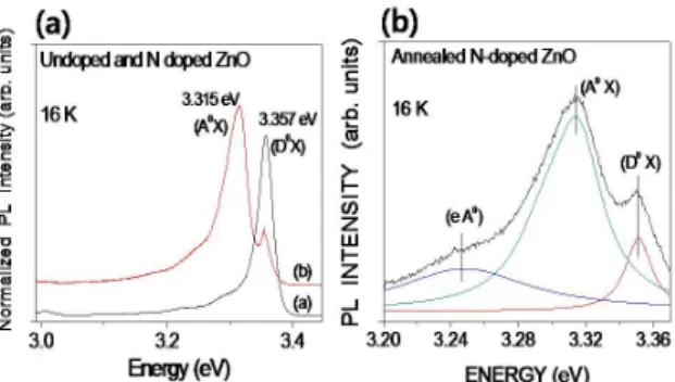
Abstract - We have grown, for the first time to our knowledge, N-doped ZnO thin films on sapphire substrate by employing novel dielectric barrier discharge in pulsed laser deposition (DBD-PLD). DBD guarantees an effective way for massive in-situ generation of N-plasma under the conventional PLD process condition. Low-temperature photoluminescence spectra of the N-doped ZnO film provided near band-edge emission after thermal annealing process. The emission peak was resolved by Gaussian fitting to find a dominant acceptor-bound exciton peak (A

0

X) that indicates the successful p-type doping of ZnO with N.

1. 서 론

ZnO has gained considerable attention as a promising material for short-wavelength optoelectronic devices, such as photodetectors, light emitting diodes, and laser diodes, due to its wide band gap of 3.37 eV and large exciton binding energy of 60 meV at room temperature.

1

Normally, undoped ZnO exhibits n-type conductivity. The realization of p-type ZnO that is considered as a key issue for more advanced application of the material has been proven difficult due to the self-compensating effect of native defects and interstitial ions.

2

Fortunately, thanks to the considerable worldwide efforts, investigations on p-type ZnO have proceeded at a rapid pace and various elements have been demonstrated as p-type dopants, including group-V and group-I elements. Among them, N appears promising candidate considering its size and energy level. However, the resultant p-type ZnO:N films are usually unstable. Recently, in order to overcome the difficulties, a theory for large-sized-mismatched group-V dopants based on first-principles calculations has been presented.

3

Also, several groups have reported p-type conductivity in ZnO by doping with large-sized-mismatched impurities, such as P, As, Ag, and Sb. Generally, the substitution of the lattice oxygen with nitrogen in ZnO has been recognized as a potential mechanism for p-type doping of ZnO, however, according to Zunger’s “practical doping rules,”

4

the p-type doping under equilibrium conditions is difficult to be achieved be cause the spontaneous compensation of the defects that yield the excessive electrons overwhelms doping pathways when the pinning energy is reached. Similar work done by Marfaing and Lusson shows that p-type doping of ZnO by the substituting nitrogen is limited by the trade-off between zinc enrichment (i.e. higher solubility) and oxygen enrichment (i.e. lower compensation of the acceptors). Even though many studies have tried to prepare the N-doped p-type ZnO, therefore, rectifying junctions, and even ZnO homojunction LEDs, they do not guarantee the reliability, stability along with efficiency of the p-type doped ZnO.

In this work, N-doped ZnO film has been grown on sapphire substrates by novel dielectric barrier discharge method in pulsed laser deposition (DBD-PLD). Importantly, it has a critical meaning in the diversification of the tools to realize the reliable and effective p-type doping of ZnO. The structural and optical properties of the N-doped p-type ZnO thin films are discussed with the results of x-ray diffraction

(XRD), x-ray photoelectron spectroscopy (XPS), and photoluminescence (PL) to verify the successful p-type doping.

2. 본 론 2.1 실험방법

N-doped ZnO thin film was prepared by the combined method of DBD and PLD by which the N-doping source was generated with the identical process condition for normal PLD process. During growth, the pressure of background gas was maintained at 350 mTorr. The c-axis sapphire substrate was used for the film synthesis. For the laser ablation in PLD, Nd:YAG laser with the laser frequency of 5 Hz, and the laser energy density of 1 J/cm

2

was used. The thickness of the resultant thin films was measured to be about 300 nm.

Thermal annealing was carried out at 800 °C for 15 min under oxygen ambient. The structural property of the samples was investigated by using XRD where a Ni-filtered Cu Kα source was used, and the binding structural properties were analyzed with XPS. The optical properties were characterized by PL with a He-Cd laser as a light source of the excitation wavelength of 325 nm and the power of 20mW.

2.2 결과 및 검토

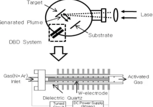
Figure 1 shows the schematic diagram of DBD equipment that is designed for the generation and the supply of active nitrogen source. Quartz tube which has a relatively high dielectric constant ( ε

r

=3.9) has been used as a dielectric barrier material in the discharge zone. A discharge electrode, tungsten (W) or molybdenum (Mo) was used as a power electrode at the center of quartz tube and aluminum radiator was used for the ground at outer quartz. To generate micro-discharge between power electrode (W or Mo) and inner wall of quartz tube, alternate current (AC) was applied between W-rod and Al-electrode. For the purpose of effective cooling originating in micro-discharge, aluminum that has a round shape with a large number of fins was added. Cooling water and cooling fan were also set up at the region of aluminum radiator. W electrode was pressed into stainless tube, which was extended to quartz tube using ultra-Torr joint to insulate another unit. AC power was supplied at the

Fig. 1. Schematic of combined DBD-PLD system and DBD system.

2009년도 대한전기학회 하계학술대회 논문집 2009. 7. 14 - 17

(2)

- 1257 -

Fig. 2. (a) X-ray dffraction patterns of undoped ZnO thin film (red) grown by conventional PLD, and annealed N-doped ZnO thin film (black) grown by DBD-PLD. (b) XPS data of N-doped ZnO thin films grown by DBD-PLD at R.T. Sample was annealed at 800 ℃ for 15 min.

stainless tube. The end quartz tube was connected to nitrogen inlet. When high-purity nitrogen gas flowed in the discharge gap through four holes of stainless tube, micro-pinning discharge between the electrodes dissociated N

2

molecules and produced active nitrogen atoms, which could be used as the N-source for the doping. Identifying the after grow of yellowish orange light, the formation of atomic nitrogen can be confirmed. AC electric power and frequency for continuous discharge reaction were determined by the gap between dielectric barrier and electrode, RF power, and gas pressure.

The system was equipped with an impedance matching with serial inductor to fit the frequency range of 200-300 kHz.

Impedance matching was achieved by tuning the frequency at constant capacitance (C) and reactance (L). With the matching network, we could get an RMS voltage between power and ground electrodes of about 3 kV. Active nitrogen species from discharge zone were supplied at the front part of PLD chamber.

Figure 2 (a) shows the comparison between the XRD patterns of N-doped ZnO films synthesized by DBD-PLD method and undoped ZnO films prepared by normal PLD method. With both cases, only one peak corresponding to the (002) plane of ZnO was observed in the pattern suggesting a high (002) preferential orientation, and no other phases were detected. Compared with the undoped ZnO films grown by PLD, the full width at half maximum (FWHM) of (002) peak of N-doped ZnO grown by DBD-PLD is increased indicating that undoped ZnO has the FWHM of about 0.4°, while N-doped ZnO has about 0.55°. It is considered that wider peak width of the N-doped ZnO film is mainly from the N incorporation. Furthermore, the peak position of (002) peak was shifted to the high angle direction. Generally, N-doped ZnO thin film is usually found to have tensile stress and shorter lattice constants, which is well agreed with the result of peak shift due to N incorporation.

To understand the origin of compensation defects, XPS was used to identify the chemical state of N atoms in N-doped ZnO. Theory predicts that N can be incorporated into ZnO by at least two different states. N atom substitution into the oxygen site of ZnO (N

O

) is a desired acceptor, and (N

2

)

O

is a N

2

molecule occupying a position on the oxygen sublattice as a shallow double donor. Figure 2 (b) illustrates N1s narrow scan spectrum for N-doped ZnO thin film grown on the sapphire substrate by DBD-PLD. One peak with maximum values at about 398 eV is observed, which corresponds to the N 1score level. The peak of the N 1s core level can be fitted into one Gaussian peak on deducting the base line, which indicates that only one chemical bonding state of N exists in the N-doped ZnO thin film. N 1s peak centered at 398 eV is generally attributed to N-Zn bonding. Therefore, it is concluded that the incorporated N in the film should exist as N

O

rather than N

Zn

. The N–Zn bond dominates in the whole spectrum for the N-doped sample, which confirms that the nitrogen mainly forms a N

O

state in ZnO.

Figure 3 (a) shows PL spectra comparing the annealed

Fig. 3. (a) Photoluminescence data of undoped ZnO grown by PLD (inset as marked (a)) and annealed N-doped ZnO grown by DBD-PLD (inset as marked (b)) measured at 16 K. (b) Desolved PL peak of the annealed N-doped ZnO fitted by Gaussian function of annealed N-doped ZnO. The sub peaks describe (D

0

X), (A

0

X) and (eA

0

), respectively.

N-doped ZnO film and undoped ZnO film. Undoped ZnO film showed dominant donor bounded exciton (D

0

X) peaks, whereas N-doped ZnO film clearly showed the acceptor bounded exciton (A

0

X) peaks. For the undoped ZnO film, a dominant near band-edge emission peak was observed at 3.357 eV. This emission is associated with the donor-bound exciton (D

0

X), which is apparently originated from the hydrogen-bound exciton denoted by I

4

in the literature. The low-temperature PL spectrum of the N-doped ZnO film significantly differs from the undoped ZnO film by exhibiting two dominant broad peaks centered at 3.315 and 3.357 eV. Many studies indicate that this peak at 3.315 eV is attributed to acceptor-bound exciton emission (A

0

X) caused by N acceptor.

In order to better understand the intrinsic p-type behavior, as shown in Figure 3 (b), fine-scanned PL spectrum was investigated for the N-doped ZnO thin film at 16 K. The figure shows Gaussian fitting to the near band-edge emission peak, consisting of three bands centered at 3.351, 3.314, and 3.248 eV, respectively. A strong emission peak is located at 3.314 eV. The position of this peak accords well with the neutral acceptor bound exciton (A

0

X) in ZnO. On the higher energy side, an obvious peak at 3.351 eV is attributed to a donor-bound exciton (D

0

X). And small peak near 3.248 eV is attributed to a free-to-neutral-acceptor (eA

0

) transitions. For (e,A

0

) emission, the peak position can be well described according to previous report as E

eA

= E

g

(T) − E

A

+ k

B

T/2, where E

A

is the acceptor energy level and k

B

is the Boltzmann constant. The obtained acceptor binding energy E

A

is 145 meV, that agrees with the value reported for N-doped ZnO, 140 meV by Ye.

5

3. 결 론

In conclusion, it was demonstrated that nitrogen can be activated for the effective doping into acceptor states in ZnO lattice using novel DBD-PLD method. This is the first time to our knowledge to demonstrate the p-type ZnO synthesis by an efficient plasma generator under the PLD process condition highlighting the in-situ doping. We expect to achieve further applications of our novel DBD system to the fields of semiconductors that require an economic, yet powerful doping tool.

[참 고 문 헌]

[1] Z. K. Tang, G. K. L. Wong, P. Yu, M. Kawasaki, A.

Ohtomo, H. Koinuma, and Y. Segawa, Appl. Phys. Lett. 72, 3270, (1998).

[2] C. G. Van de Walle, Phys. Rev. Lett. 85, 1012, (2000).

[3] S. Limpijumnong, S. B. Zhang, S.-H. Wei, and C. H. Park, Phys. Rev.Lett. 92, 155504, (2004).

[4] A. Zunger, Appl. Phys. Lett. 83, 57, (2003).

[5] B. P. Zhang, N. T. Binh, Y. Segawa, Y. Kashiwaba, and

K. Haga, Appl. Phys. Lett. 84, 586, (2004).

수치

Fig.  1.  Schematic  of  combined  DBD-PLD  system  and  DBD  system.
Fig.  2.  (a)  X-ray  dffraction  patterns  of  undoped  ZnO  thin  film  (red)  grown  by  conventional  PLD,  and  annealed  N-doped  ZnO  thin  film  (black)  grown  by  DBD-PLD

참조

관련 문서