통신위성우주산업연구회논문지 제 권 제 호6 1 (K6-1-5)
28
For Radio frequency microelectromechanical system (RF-MEMS) switches offer great potential benefits over PIN diodes and transistor switches in aspect to low insertion loss, highisolation, and negligible power consumption.[1] Switching is accomplished by the mechanical deflection of a suspended structure and the deflection can be obtained using electrostatic, magnetostatic,
piezoelectric, or thermal actuation.[2] To date, the majority of MEMS switches employ electrostatic actuation.[3] However, the actuation mechanism is a nonlinear and usually requires high voltages to operate. These important drawbacks are undesired considering their application in handheld wireless communication systems like mobile phones.[4,5]
In contrast, piezoelectric actuation is a linear, can operate lower voltages. In addition, the mechanism allows the design of larger contacts for high power capability as well as improved reliability due to
압전 MEMS 스위치 구현을 위한 DLC 구조층에 관한 연구
황현석*, 이경근**, 유영식***, 임윤식****, 송우창***** 정회원
DLC Structure Layer for Piezoelectric MEMS Switch
Hyun Suk Hwang*, Kyonggun Lee**, Young Sik Yu***, Yun-Sik Lim****, Woochang Song***** Regular Members
요 약
본 논문에서는 d33 모드로 구동하여 우수한 성능을 가지는 RF-MEMS 스위치의 구현을 위한 희생층과 구조층의 조합으로서 와 포토레지스트를 제안하였다 포토레지스트의 경화현상을 방지하기 위하여 구조층은 상온에서 방법을 이용
DLC . DLC RF-PECVD
하여 증착하였다 그리고. PZT 압전층은 RF 마그네트론 스퍼터링 방법을 이용하여 상온에서 구조층 위에 증착하였으며 희생층의, 제거 후 결정화를 위하여 급속 열처리(RTA) 장비를 이용하여 후 열처리하였다. PZT의 결정화 과정과DLC의 기계적 성질의 변화 를 다양한 온도조건에 따라 분석한 결과 DLC는 PZT의 결정화 온도까지 영률과 강도면에서 우수한 특성을 나타냄을 확인하였다. 또한 포토레지스트를 사용함으로서 공정을 단순화하고 낮은 비용으로 제작이 가능하였다.
Key Words : diamond like carbon (DLC), structure layer, piezoelectric, MEMS, switch
In this paper, a new set of structural and sacrificial material that is diamond like carbon (DLC)/photoresist for high performance piezoelectric RF-MEMS switches which are actuated in d33 mode is suggested. To avoid curing problem of photoresist sacrificial layer, DLC structure layer is deposited at room temperature by radio frequency plasma enhanced chemical vapor deposition (RF-PECVD) method. And lead zirconate titanate (PZT) piezoelectric layer is deposited on structure layer directly at room temperature by rf magnetron sputtering system and crystallized by rapid thermal annealing (RTA) equipment. Particular attention is paid to the annealing of PZT film in order to crystallize into perovskite and the variation of mechanical properties of DLC layer as a function of annealing temperature. The DLC layer shows good performance for structure layer in aspect to Young’s modulus and hardness. The fabrication becomes much simpler and cheaper with use of a photoresist.
서일대학교 전기과
* ([email protected]), **성균관대학교 전기전자 및 컴퓨터공학과([email protected]), ***여주대학 전기과, 여주대학 방송제작 연예과
****
이 논문은 교육과학기술부의 재원으로 시행하는 한국과학재단의 연구지원프로그램으로 지원받았습니다 연구과제 관리코드
" .( : 2010-0025245)"
접수일자: 2011년 1월 31일 수정완료일자, : 2011년 2월 18일 최종게재확정일자, : 2011년3월 8일
압전MEMS스위치 구현을 위한DLC구조층에 관한 연구
29 mitigated stiction effects.[4] Lead zirconate titanate
(PZT) is a representative piezoelectric material and a number of surface micromachined actuator utilizing PZT films have been reported for its high piezoelectric coefficient.[5] Recently, for high performance piezoelectric RF-MEMS switches, PZT thin film is deposited on the structure layer directly which is used to increase deflection as well as support structure when the PZT is poled in the transverse direction and actuated in the d33 modes.[4,5] It is well known that the magnitude of the d33 coefficient of PZT is about twice the d31 coefficient.[5]
The piezoelectric MEMS switches are largely composed of piezoelectric layer, structure layer and electrode. And it is important that choose a set of structural and sacrificial material for simpler and cheaper process. The common sets are polycrystalline silicon/silicon dioxide, polyimide /aluminum, Silicon nitride/polycrystalline silicon and tungsten/silicon dioxide, etc.[6]
In this paper, we present a set of structural and sacrificial material that is DLC/photoresist for high performance PZT RF-MEMS switches. A photoresist sacrificial layer has many advantages that is easy to coat, easy to dissolve, can be patterned and is compatible with the materials and processes used in conventional IC manufacturing.[7] But the entire process must to be done under 200oC which is curing temperature. DLC film can be prepared at relatively low temperatures by radio frequency plasma enhanced chemical vapor deposition (RF-PECVD) method, which has been widely used for the synthesis of DLC thin film because it uses standard plasma processing technology that allows the simple and relatively inexpensive low- temperature coating of a range of temperature sensitive substrates and can be uniformly coated on the substrate of different shapes and sizes[8] and easily control the DLC properties by controlling the hydrogen contents in the film.[9] Therefore DLC film is suitable for structure layer which process use photoresist as a sacrificial layer.[10] And this fabrication of MEMS becomes much simpler and cheaper with the use of a photoresist as a sacrificial layer. And particular attention is paid to the annealing of PZT film in order to crystallize of PZT film into perovskite maintaining the properties of DLC film.
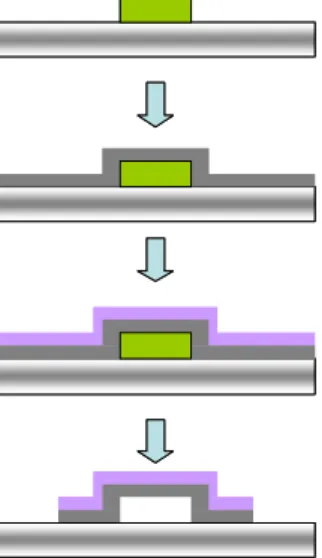
The basic process steps are illustrated in figure 1.
(1) Photoresist coating
& patterning
(2) DLC deposition
(3) PZT deposition
(4) Patterning & Releasing (1) Photoresist coating
& patterning
(2) DLC deposition
(3) PZT deposition
(4) Patterning & Releasing
Figure 1. Basic process steps for fabricate structure
First, a photoresist sacrificial layer is spun on a substrate and patterned by using standard lithography procedure and photoresist fabrication techniques. The entire process until the removal of the sacrificial layer is kept below 180oC. Therefore there is no heating process except by plasma.
Next, methane and nitrogen gases are then introduced into the reaction chamber to grow the films at room temperature by RF-PECVD method.
(step 2) The substrate is heated only by the plasma during the film growth and the deposition time was kept as 5 min 30 sec for every sample. The deposition condition is shown Table 1.
In step 3, PZT thin film is prepared by rf magnetron sputtering system using Pb1.1(Zr0.52
Ti0.48)O3commercial ceramic target. Table 1 shows the deposition condition of PZT thin film.
Room Temperature Substrate temperature
5 min 30 sec Deposition time
Electrode to substrate 7 cm distance
150 W RF power
1 Torr Working pressure
CH4: 20 sccm H2: 80 sccm Deposition gas
Room Temperature Substrate temperature
5 min 30 sec Deposition time
Electrode to substrate 7 cm distance
150 W RF power
1 Torr Working pressure
CH4: 20 sccm H2: 80 sccm Deposition gas
통신위성우주산업연구회논문지 제 권 제 호6 1
30
120 min Deposition time
400 nm Film thickness
Room temperature Substrate temperature
125 W RF power
16 : 4 Ar : O2flow rate
5×10⁻³Torr Working pressure
Si (100) Substrate
2 inch 10% access PZT ceramic target Target
120 min Deposition time
400 nm Film thickness
Room temperature Substrate temperature
125 W RF power
16 : 4 Ar : O2flow rate
5×10⁻³Torr Working pressure
Si (100) Substrate
2 inch 10% access PZT ceramic target Target
Finally, each layer is pattered and the structure is released. And then the structure is annealed by rapid thermal annealing (RTA) equipment for 180 seconds in order to crystallize of PZT film into perovskite.
2. Application on Genetic Algorithm
The surface morphology and properties of DLC and PZT thin films are analyzed using an atomic force microscope (AFM), X-ray diffraction (XRD).
Toinvestigate change of the film properties according to annealing temperature and to decide PZT annealing condition which process is needed tocrystallize of PZT film into perovskite. The experiment is done by RTA equipment after DLC deposition step in oxygen ambient as a function of annealing temperature from 300 to 900℃ in steps of 200 . The hardness and Young’s modulus of the℃ film are analyzed using a nano-indenter.
. Result and Discussion
Ⅲ
The AFM images of each layer is shown figure 2.
DLC thin film is good for under layer in aspect to surface roughness. The value of surface roughness (RMS) of DLC film and PZT film deposited on DLC layer are 0.22 nm and 1.05 nm, respectively.
(a) (b)
(a) (b)
Figure 2. AFM images of films : (a) DLC film and (b) PZT film
Fig. 3 shows the hardness and Young’s modulus of
as-deposited and annealed DLC films at 300, 500, 700, and 900℃ with a nano-indenter measurement.
The hardness abruptly decreases from 20.3 to 12.7 GPa between500 and 700 . The post annealing℃ treatment results in the increase of graphitic fraction in the film and clustering of sp2 bonded carbon. DLC structure layer has strong advantages of hardness and Young’s modulus in spite of decreasing their values.
300 500 700 900
10 12 14 16 18 20 22
Hardness Young's modulus
Annealing temperature [oC]
Hardness [GPa]
90 105 120 135 150 165 180 195
Young's modulus [GPa]
As-depo.
Figure 3. Hardness and Young’s modulus of DLC films as a function of annealing temperature
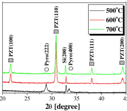
The XRD pattern of the PZT thin film is shown in Figure 4. The perovskite structure of PZT thin films is obtained by RTA treatment for 180 seconds over 600oC. We have reported that the oriented sample by the RTA treatment can improve the electrical property of PZT thin film.
20 25 30 35 40 45
Pyro(222) Si(200)
PZT(100) PZT(200)
Intensity [a.u]
2θ [degree]
500oC 600oC 700oC
Pyro(400)
PZT(110) PZT(111)
Figure 4. XRD patterns of PZT thin films as a function of annealing temperature
. Conclusion
Ⅳ
A new set of structural and sacrificial material
압전MEMS스위치 구현을 위한DLC구조층에 관한 연구
31 that is DLC/photoresist for PZT RF-MEMS switches
has been suggested. Photoresist sacrificial layer has many advantages that is easy to coat and dissolve but the process must to be done at low temperature to avoid photoresist curing. DLC film is prepared at room temperature by RF-PECVD method and shows good performance for structure layer in aspect to Young’s modulus and hardness. The PZT film which is deposited on DLC layer is well crystallize into perovskite structure. The fabrication of micromechanical systems becomes much simpler and cheaper with use of a photoresist.
References
[1] V. J. Varadan, "RF MEMS AND THEIR APPLICATIONS", John Wiley & Sons Ltd, Chichester, CH. 1., 2003.
[2] G. M. Rebeiz, "RF MEMS THEORY, DESIGN, AND TECHNOLOGY", John Wiley & Sons Ltd, New Jersey, CH. 1., 2003.
[3] K. E. Petersen,“Microelectromechanical Membrane Switches on Silicon”, IBM J.Res. Dev. 23, pp.
376-385 1979.
[4] Q. Q. Zhang, S. J. Gross, S. Tadigadapa, T. N.
Jackson, F. T. Djuth, and S. Trolier-McKinstry,
"Lead zriconate titanate for d33 mode cantilener actuators", Sens. Actuators, A 105, pp. 91-97, 2003.
[5] S. J. Gross, S. Tadigadapa, T. N. Jackson, S.
Trolier-McKinstry, and Q. Q. Zhang,
"Lead-irconate-titanate-based iezoelectric micromachined switch", Appl. Phys. Lett., 83, pp. 174-176, 2003.
[6] V. J. Varadan, "RF MEMS AND THEIR APPLICATIONS", John Wiley & Sons Ltd, Chichester, CH. 2., 2003.
[7] Z. Cui and R. A Lawes, "A new sacrificial layer process for the fabrication of micromechanical systems", J. Micromech. Microeng., 7, pp.
128-130, 1997.
[8] T. Michler, M. Grischke, I. Traus, K. Bewilogua, and H. Dimigen, "DLC Films deposited by bipolar pulsed DC PACVD", Diam. Relat. Mater. 7, pp.
459-462, 1998.
[9] C.-L. Cheng, C.-T. Chia, C.-C. Chiu, C.-C.
Wu, and I.-N. Lin, "Hydrogen effects on the post-production modification of diamond-like carbon produced by pulse laser deposition",
Diam. Relat. Mater. 10, pp. 970-975, 2001.
[10] J. C. Orlianges, A. Pothier, D. Mercier, P.
Blondy, C. Champeaux, A. Catherinot, M. I. De Barros, and S. Pavant, "Application of aluminum oxide and ta-C thin films deposited at room temperature by PLD in RF-MEMS fabraication", Thin Solid Films, 482, pp. 237-241, 2005.
저 자
황 현 석 (Hyun Suk Hwang) 정회원
년 월 성균관대학교 전기전자 2007 8 :
및 컴퓨터공학과 박사 년 월 현재 서일대학 전기과
2009 3 ~ :
전임강사
관심분야 통신부품
< > , USN
이 경 근 (Kyonggun Lee)
년 월 한국외국어대학교 학사 2010 2 :
년 현재 성균관대학교 전기
2010 ~ :
전자및컴퓨터공학과 석사과정
관심분야 임베디드컴퓨터 통신시스템
< > ,
유 영 식 (Young Sik Yu)
년 월 성균관대학교 공과대학 1999 2 :
전기공학과 박사 년 현재 여주대학 전기과 교수
1993 ~ :
관심분야 고분자 절연재료 태양에
< > ,
너지
임 윤 식 (Yun-Sik, Lim)
년 성균관대학교 전기공학과 1998 :
공학박사
년 현재 여주대학 방송제작
1998 ~ :
연예과 부교수
관심분야 무선통신 방송기술분야
< > ,
송 우 창 (Woochang Song)
년 월 성균관대학교 공과대학 2001 8 :
전기공학과 박사 년 현재 강원대학교 삼척캠퍼
2010 ~ :
스 전기공학과 교수
관심분야 고분자 절연재료 태양
< > ,
에너지