KEPCO Journal on Electric Power and Energy, Vol. 2, No. 2, June 2016
Manuscript received August 28, 2015, revised May 3, 2016, accepted May 4, 2016 ISSN 2465-8111(Print), 2466-0124(Online), DOI http://dx.doi.org/10.18770/KEPCO.2016.02.02.223
This paper is licensed under a Creative Commons Attribution-NonCommercial 4.0 International License. This paper is available online at http://journal.kepco.co.kr 223
Experimental Study for Gate Trap and Generation Current using DCIV Method
Young Kwon Kim
*, Dong Bin Lee
*, Won Hyeok Choi
*, Taesik Park
**, Myoung Jin Lee
*†
*
School of Electronics and Computer Engineering, Chonnam National University, Gwangju, 500-757, Korea
**
Department of Electrical Engineering, Mokpo National University, Jeollanam-do, 534-729, Korea
† [email protected]
Y. K. Kim and D. B. Lee have contributed equally to this work
Abstract
The newly proposed analysis method using a direct-current current-voltage (DCIV) simulation is introduced for investigating leakage current composing MOS transistor. From comparing the density and location of traps using DCIV method and investigating the leakage current of gate channel transistor, we proposed the graphical analysis method to correlate the DCIV current and leakage mechanism by the traps. And, our graphical method intuitively explains that leakage current in MOS transistor is well correlated with the DCIV current of the MOS transistor arrays due to two kinds of traps created by Fowler-Nordheim (F-N) stress and Hot carrier stress, respectively.
Keywords : MOS transistor, DCIV, FN and Hot carrier stress
1. INTRODUCTION
The generation current caused by the traps is the most important parameter which determines the off-characteristics in the Metal Oxide Semiconductor Field Effect Transistor (MOSFET).
The lateral direct-current current-voltage (DCIV) method has been introduced as one of the indirect methods to detect the density and location of defect by measuring the base current under the bipolar operation mode of the MOSFET. In other words, the physical location and the quantity of the defects may be discovered by observing the dependence of the base current on the gate voltage [1]-[5]. In this work, the well established DCIV method is utilized to investigate the MOS transistor and 2D device simulation is also used to analyze the generation leakage mechanism [6].
First, we show that the DCIV results on the MOS transistor are shown to explain the several peaks of the base current owing to traps and to look into the location of traps which are created by two kinds of stresses (F-N and Hot carrier stresses).
II. THE RESULTS OF DCIV FOR THE EFFECT OF TRAPS CAUSED BY FN AND HOT CARRIER STRESSES
The MOS transistor with the channel length and width of 0.2
m and 10 m has been used in this study. The schematic of lateral DCIV method is shown in Fig. 1. To measure the dependence of the base current on gate voltage, we apply -0.3 V and 0.5 V to V
SBand V
DBrespectively. Thus, we can consider drain-channel-source as emitter-base-collector.
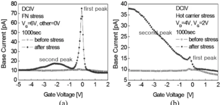
Fig.2 shows the measured base current according to gate voltage, and several peaks are found. To confirm what the cause
of peak is, we induce two kinds of stress to the MOS transistor.
After the F-N stress is induced, two peaks are occurred, as shown in Fig. 2(a).
It has been known that first peak is caused by interface traps in the channel, and second peak by interface traps in the gate overlapped region [7]. When the number of electron equals that of hole, i.e. E
i=(E
Fn+E
Fp)/2, the recombination current occurred in this region mainly contributes to the magnitude of the base current in DCIV measurement. Fig. 3 shows that the region where maximum recombination occurs varies with gate voltage. In the case of second peak in Fig. 2, recombination was occurred by trap assisted tunneling mechanism.
And both E
i=(E
Fn+E
Fp)/2 line and electric field contour
decide the region of maximizing recombination. Therefore, the
region moves from interface to deeper location in inner drain area
as negatively increasing gate voltage, as shown in Fig. 4. After
Hot carrier stress is induced as shown in Fig. 2(b), the increase of
second peak is remarkable. It has been known that F-N stress
Fig. 1. Schematic illustrations of the DCIV measurement. We apply -0.3 V and 0.5 V to VSB and VDB to consider drain-channel-source as emitter- base-collector, respectively.Young Kwon Kim, et al.: Experimental study for gate trap and generation current using DCIV method
224
creates the interface traps in the channel and gate overlapped region [8][9]. These kinds of traps contribute to first and second peak in base current, respectively. But in the Fig. 2(b), the magnitude of second peak with Hot carrier stress continued to increase with negative gate bias contrary to that with F-N stress.
Hence, it is obvious that both interface trap and the bulk trap in the gate overlapped region contribute to the magnitude of second peak. As a consequence, F-N stress create only interface trap, while hot carrier stress create not only interface trap but also inner bulk traps.
III. THE ANALYSIS OF THE RELATION BETWEEN THE DCIV CURRENT AND DRAM LEAKAGE
CURRENT
Second, we analyze the relationship between the DCIV current and the MOS transistor generation leakage current caused by traps. In each case, both generation and recombination are occurred by the trap assisted tunneling which arise from the trap in the gate-drain overlapped region [10]. Fig. 5 shows that each leakage current in device with F-N stress and Hot carrier stress depend on drain voltage respectively. The device with the interface traps created under F-N stress even shows high leakage
current level irrespective of drain voltage.
On the other hand, the leakage current of the device under Hot carrier stress is very dependent on the drain voltage. These are analogous to the dependence of DCIV current on gate voltage in Fig. 2(b). The device with hot carrier stress in Fig. 2(b) showed characteristics that the base current continues to increase with negative gate bias, too. As a result, the second peak in the base current of DCIV in Fig.2 is related to the leakage current in the
(a) (b)
Fig.2. Characteristics of DCIV current for. (a) with F-N stress, (b) with hot carrier stress. The second peak in (a) is caused by interface trap, while that in (b) is due to inner bulk trap in the gate-drain overlapped region.
Fig.3. The region in which maximum recombination occurs varies with gate bias. As electric field in the gate-drain overlapped region increase with negative gate bias, trap assisted tunneling through inner bulk trap contribute to recombination current in DCIV.
(a) (b)
Fig. 4. In DCIV, both Ei=(EFn+EFp)/2 line and Electric field contour decide the region which in maximum recombination occur. We confirm that inner bulk trap contributes to maximum base current at VG = -5 V through 2D simulation of structure with uniform trap distribution.
Fig. 5. Dependence of leakage current on drain voltage between F-N stress and hot carrier stress is different.
Fig. 6. Energy band is drawn perpendicular to channel in the gate-drain overlapped region. There are two kinds of path. One is path through interface trap, and the other is path through inner bulk trap.
KEPCO Journal on Electric Power and Energy, Vol. 2, No. 2, June 2016
225
MOS transistor. We can explain these phenomena through the figure of energy band in Fig. 6. When trap assisted tunneling occur through the interface trap, the movement of electron from trap to conduction band is enhanced by electric field, while that from valence band to trap is not enhanced. And this trap assisted tunneling mechanism through the interface trap is limited by path from valence band to interface trap. When trap assisted tunneling occur through the inner bulk traps, both the movement of electron through each path are enhanced by electric field. These mechanisms explain different dependence of leakage current on electric field.
IV. CONCLUSIONS
We analyze the cause of the generation leakage current related with the MOS transistor using DCIV method. We show that F-N and Hot carrier stress create traps in different location, which generate the different leakage mechanism and dependence on electric field.
ACKNOWLEDGMENT
This research was supported by Basic Science Research
Program through the National Research Foundation of Korea (NRF) funded by the Ministry of Education (2015R1D1A1A0106 1081).
REFERENCES
[1] A. Neugroschel, C.-T. Sah, M. Han, M.S. Carroll, T. Nishida, J.T.
Kavalieros, Y. Lu, IEEE Trans. Electron Devices 42. 1995, p1657.
[2] E. X. Zhang, D. M. Fleetwood, S. A. Francis, C. X. Zhang, F. El- Mamouni, R. D. Schrimpf, 2011 International Semiconductor Device Research Symposium, 2011, pp1-2.
[3] Y. He, G. Zhang, L. Han, X. Zhang, IEEE Electron Device Letters 33, 2012, pp1435.
[4] Y. He, G. Zhang, X. Zhang, IPFA, 2014, pp264-267.
[5] M. Bina, Th. Aichinger, G. Probegen, W. Gos, T. Grasser, 2011 IEEE IIRWFR, 2011, p27.
[6] ATLAS User’s Manual, SILVACO International, 2015.
[7] B.B. Jie, W.K. Chim, M.-F. Li, K.F. Lo, IEEE Trans. Electron Devices 48, 2001, p913.
[8] J.-D. Lee et al., IEEE Trans. Electron Devices 4, 2001, p110.
[9] M. J. Lee, S. J. Jin, C-K. Baek, S.M. Hong, S.Y. Park, H.H. Park, S.D. Lee, S.W. Chung, J.G. Jeong, S.J. Hong, S.W. Park, I.Y. Jung, Y.J. Park and H.S. Min, IEEE Trans. Electron Devices 54, 2007, p3325.
[10] G.A.M. Hurkx, D.B.M. Klaassen, M.P.G.. Knuvers, IEEE Trans.
Electron Devices 39, 1992, p33.