A High Current Efficiency CMOS LDO Regulator with Low Power Consumption and Small Output
Voltage Variation
Behnam Samadpoor Rikan*, Hamed Abbasizadeh*, Ji-Hun Kang*, Kang-Yoon Lee*★
Abstract
In this paper we present an LDO based on an error amplifier. The designed error amplifier has a gain of 89.93dB at low frequencies. This amplifier’s Bandwidth is 50.8MHz and its phase margin is 59.2˚.
Also we proposed a BGR. This BGR has a low output variation with temperature and its PSRR at 1 KHz is -71.5dB. For a temperature variation from -40˚C to 125˚C we have just 9.4mV variation in 3.3V LDO output. Also it is stable for a wide range of output load currents [0-200mA] and a 1µF output capacitor and its line regulation and especially load regulation is very small comparing other papers. The PSRR of proposed LDO is -61.16dB at 1 KHz. Also we designed it for several output voltages by using a ladder of resistors, transmission gates and a decoder. Low power consumption is the other superiority of this LDO which is just 1.55mW in full load. The circuit was designed in 0.35µm CMOS process.
Key words: Low-dropout(LDO) Regulator, Bandgap Reference(BGR), Error amplifier, Load Regulation, Line Regulation
* College of Information and Communication Engineering, Sungkyunkwan University
★Corresponding author [email protected], 031-299-4954
※ Acknowledgment
"This research was supported by the MSIP(Ministry of Science, ICT&Future Planning), Korea, under the ITRC(Information Technology Research Center)"
Support Program : "This work was supported by IC Design Education Center(IDEC)"
Manuscript received Jan. 15, 2014; revised Feb.
I. Introduction
These days power management is an important consideration in portable electronic devices such as cellular phones, hand-held computers, and particularly implanted wireless biomedical chips.
The purpose of power management is to reduce power consumption and increase the battery life.
Low-dropout(LDO) regulators are widely used alone in many integrated power management circuits but are also used as post regulators of switching converters, as they can provide wideband regulated low noise supply voltage for noise-sensitive analog and RF loads. Traditional linear LDO regulators usually consist of a two-stage error amplifier, a power output stage and a negative feedback loop. The error amplifier detects the error between the reference and the output voltage. There are several performance metrics to be fulfilled when designing an LDO, such as closed-loop stability for a wide range of loads, static regulation in front of input voltage and load variations, and fast rejection of steep transient load variations [1, 2].
Operational amplifiers (OP-AMPS) have become one of the core components in analog and mixed signal (AMS) design. The proposed error amplifier here is a two stage high speed CMOS op-amp. The design procedure involves designing the bias circuit, the differential input pair, and gain stage [3].
As we mentioned the error amplifier detects the error between the reference and the output voltage. The reference voltage is produced by a Bandgap Reference(BGR). Precision BGRs are critical building blocks for a variety of analog and mixed signal electronic devices such as data converters, PWM controllers, oscillators, operational amplifiers, linear regulators and PLLs.
Undoubtedly the reference voltage accuracy plays a significant part in determining the performance of all subsequent circuits, which depend on an accurate and stable reference [4,5].
All these parts gathered together and make an LDO. Conventional LDOs just give an output which’s variation with temperature is low.
Unfortunately most of the designed LDO's can't provide all of the LDO performance metrics together and each of them has a low performance in one aspect. And also their load current variation is in small range and they can't suffer high load currents. In this paper we propose an LDO with high stability for line, load and temperature variations. The load current has been increased comparing other papers and also this LDO can provide several needed voltages at the output.
In section II of this paper we present the proposed BGR. Section III describes the proposed error amplifier and its characteristics. Then in section IV we will see the structure of LDO.
Finally the simulation results will be shown in section V.
II. Bandgap Reference
To generate a stable voltage against process and temperature variations, a BGR circuit is adopted.
BGR circuit was first proposed by Widlar [6] and
was further developed by Brokaw [7], that are most commonly used for all analog circuits for providing reference voltages. We will use it in our LDO [1,8]. The conventional BGR structure is shown in Fig.1. which is composed of CMOS opamp, BJTs and resistors.
The relation between the diode current and VBE
voltage can expressed as:
×
or
× ln
Fig. 1. Conventional BGR circuit
Here , and × is Boltzmann’s constant and × is electronic charge. ∆ is the forward voltage difference between Q1 and Q2 transistors for different current densities.
∆ × ln
In conventional BGR circuit, and nodes are controlled by opamp circuit and BGR output voltage VREF is given by
×ln
The BGR here uses the same structure as conventional BGRs (Fig.2.). Transistors M1-M8 are op-amp transistors. A start up circuit (M11-M14) also added to ensure BGR's start up situation. Proportional to absolute temperature (PTAT) current is created through M9 and M10 and temperature independent voltage is created
by using R4 in VREF. To overcome the supply dependence caused by channel-length modulation of MOS devices, we have used cascade topology for both NMOS and PMOS transistors. Also R2 and R3
sustain proper voltages to allow MOSFETs to remain in saturation [8].
Fig. 2. BGR proposed to use as VREF in LDO This BGR produces 1.2V for the error amplifier of LDO. It has a very small variation for temperature sweep of -40˚C to 125˚C which is important to be used as reference voltage of LDO. Also high PSRR is the other priority of this BGR which is so important parameter in these days BGR and LDO design. Table1 shows this BGR’s characteristics.
Table 1. BGR circuits performance parameters This Work [4]
Reference Output
Voltage 1.202 V 1.23V
Voltage Variation
for -40˚C to 125˚C ±0.1325% ±0.1%
PSRR
-72.5dB@
100Hz -71.5dB@
1KHz
-31dB
@10Hz
Current
Consumption 42.8 uA 180uA
III. Error Amplifier
The op-amp design at schematic level is mainly divided into three main parts, the biasing circuit, the input differential pair and gain stage. In this paper we propose a two stage op-amp with the bias circuit and a load capacitor CL as shown in Fig.3.
[3].
For a good performance of LDO this amplifier should have high gain and proper phase margin.
Gain of this op-amp is
×
Av1 is the first stage or differential input stage’s gain. The transistor M9 and M10 are the p-channel input pair and the M11 and M12 are the n-channel active load current mirrors. M13 and M14 are the biasing transistors. The differential pair is active loaded with the NMOS current mirror.
Fig. 3. two stage op-amp with load capacitor CL
So the differential gain of the differential pair is given by
Also we have gain stage, which is the second stage of two stage op-amp. Gain stage, is an n-channel common source amplifier, active loaded
with the PMOS current source. The gain of this stage is
A miller compensation capacitor is added between the input and the output of the gain stage so as to move the pole lowest in frequencies to lower frequencies and the one at high frequency to higher frequencies and achieve more stability at the cost of reduced speed. To get required GBW [9, 10] are used
Where fun is the GBW and Cc is the miller compensation capacitor and controls the dominant first pole.
Resistor Rc is connected in series with Cc to cancel the right half plane zero altogether[10],
Also the value of Rc is increased to move the zero further into left half plane.
Table2 shows this amplifiers performance parameters.
Table 2. Results for proposed error op-amp This work [3]
Open Loop Gain 89.93 dB >90dB Bandwidth 50.77 MHz 57.01MHz
Phase Margin 59.2˚ 56˚
Cc 800 fF 800fF
Rc 1.2K Ohm 8K ohm
CL 100 fF 10pF
IV. Low Dropout Regulator
Block diagram of proposed LDO is shown in Fig.4.
It is composed of a BGR, an error amplifier, a power MOS (MP) and a voltage divider composed of R1 and R2. More than 200mA Iload and 1uF
capacitor is used for full load situation in our simulations.
As we mentioned, Mp is a power transistor so its aspect ratio is larger than other transistors to provide 200mA load current [11].
To get several fixed output voltages (not only 3.3V output voltage) as shown in Fig.4. we replaced R1 with a ladder of 8 resistors, so according to voltages of Table3, we can get the needed output from the related node. To control the output voltage we use 8 transmission gates and control them with a 3×8 decoder.
Figure of Merit (FOM) can be calculated as below
×
where
×∆
And IQ is the current passing through R2 [11,12].
Fig. 4. Block diagram of proposed LDO
Table 3. Output voltages control bits Control bit
<2:0> VOUT(V)
000 3.61
001 3.53
010 3.45
011 3.38
100 3.31
101 3.24
110 3.18
111 3.12
V. Simulation Results
The proposed LDO topology has been designed and simulated in 0.35µm CMOS process. The simulations have been done in full load and for other load situations we will even have better results. These results are for 3.3V output voltage with 220mA load current and 1µF output capacitor and the performance for all of the other output voltages in Table3 will be the same.
Fig. 5. Error amplifier’s gain and PM First of all we can see the error amplifier gain and phase margin in Fig.5. According to the simulations, we got to the gain of almost 90dB and 59.2˚ phase margin and 50.77MHz bandwidth.
These results shows this error amplifier can be used in LDO and it will have proper performance.
Line regulation and load regulation of proposed LDO are shown in Fig.6. and Fig.7. respectively.
As we can see in Fig.6. the line regulation for this LDO is 1.937 mV (for 4.7 < VDD < 5.7).
Fig. 6. Line Regulation
This means that if our VDD have 1V variation the output voltage will vary less than 2mV. This shows LDO is stable for supply voltage variations and it is important issue in LDO design.
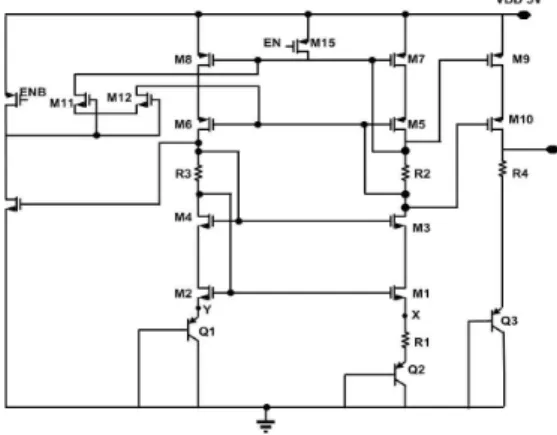
Also load regulation of this LDO is 174.334µV for 0<ILOAD<200mA, which is considerably low, comparing other works. It means we can get a large range of current in the output without so much changes in the performance and so LDO is stable for this range of load current variation. This is one of the priority of this work which can suffer comparable large ranges of load currents comparing other works.
Fig. 7. Load Regulation
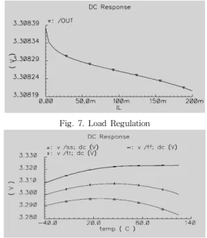
Fig. 8. Output voltage variation of LDO with temperature variation in different corners
Fig.8. shows output voltage variation with temperature. As we can see, for -40˚C to 125˚C temperature variation, we have just 9.4mV output voltage variation in Typical state. It shows the stability of the circuit to the temperature variation.
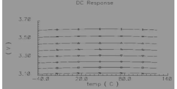
In Fig.9. we can see the 8 different outputs of the LDO. These outputs are stable for temperature variations and line and load regulations as 3.3V output node does. These 8 voltages can be obtained using a resistor ladder, transmission gates and 3×8 decoder.
Fig. 9. Different output variations of LDO with temperature variations
In Fig.10. the output voltage variation of the BGR for temperature variation has been shown. We can see the variation is small in all 3 shown corners. It is important for BGR to be stable for temperature variations which we can see in our design.
Dropout voltage of the LDO for output of 3.3V is 3.32V as shown in Fig.11. It means that for VDD voltages over 3.32V we can get the output voltage of 3.3V.
Fig.12. shows PSRR of proposed BGR and LDO respectively. High PSRR is very important issue for the good performance of the LDO. As we can see until 1KHz we have almost –61dB PSRR which shows high performance of this LDO.
Current consumption of BGR and LDO are 42.68µA and 267.14µA respectively, so power consumption of this LDO is 1.55mW.
Settling time of circuit is 141µs and FOM is 0.33nS.
Table4 presents performance summary. We should emphasize again that load current of this LDO can be even more than 200mA. It has high PSRR and low power consumption. Also it is stable for line,
load and temperature variations in high performance.
Fig.13. shows the layout of the proposed LDO. The total area is 0.1mm2 and the post simulation results confirm our simulation results.
Fig. 10. Output Voltage variation of BGR with temperature variation in different corners
Fig. 11. Dropout voltage of LDO
Fig. 12. PSRR of proposed LDO and BGR
Fig. 13. Layout of LDO and BGR
Table 4. Performance summary and comparison with recently reported LDO simulation results
[13] [14] [15] [16] [12] [17] [2] This Work
Technology[um] 0.5 0.35 0.09 0.35 0.35 0.25 0.35 0.35
Iload[mA] 160 200 100 50 50 50 100 220
Vin[V] 3.3 2-5.5 1.2 1.2-1.5 1.05-3.5 2-2.5 3-5 3.32-5
Vout[V] 2.8 1.8 0.9 1 0.9 1.5-1.97 2.8 3.3
Compensation
Cap.[pF] 5 10 × × × N.A. × 1
Output Cap.[uF] 2.2 1 0.0006 1 1 0.05 1 1
Iq[mA] 25 20-320 6000 95 4.05-164 100 59-189 120
PSRR[dB] N.A. 45@20KHz N.A. N.A. 50 45@30KHz 56 >50@10KHz
Load Reg.[mV/mA] 1.25 0.17 N.A. 0.28 N.A. 0.08 0.025 <0.01
Line Reg.[mV/V] N.A. 2 N.A. 18 1.061 N.A. 13.5 1.93
Current efficiency[%] N.A. 99.8 94.3 99.8 99.67 99.8 99.8 99.85
△Vout[mV] 200 54 90 30 6.6 15 3 137
TR[us] 2.75 0.27 0.0054 0.6 0.132 0.03 0.03 0.62
VI. Conclusion
An LDO based on an error amplifier is presented in this paper. With a ladder of resistors and a 3×8 decoder, we get 8 different output voltages. The circuit is stable for a wide range of load currents [0-200mA]. Also for source voltage and temperature variations the circuit shows high stability. For temperature variations, the maximum output voltage variation is 9.38mV. PSRR of this LDO in DC is -62.3dB and in 1 KHz is –61.2dB which shows high performance. The power consumption is 1.55mW.
References
[1] C. Wang, R. Kuo, T. Tsai, A high precision dropout regulator with nested feedback loops, Microelectronics Journal 42 (2011) 966-971.
[2] A. Saberkari, E. Alarcon, Sh.B. Shokouhi, Fast transient current-steering CMOS LDO regulator based on current feedback amplifier. Integer.VLSI J.46 (2013) 165-171.
[3] Y.M. Qureshi, Design and Layout of Two Stage High Bandwith Operational Amplifier, World Academy of Science, Engineering and Technology 71 2012.
[4] X. Ming, Y. Ma, Z. Zhou, B. Zhang, A High-Precision Compensated CMOS Bandgap Voltage Reference Without Resistors, IEEE
Trans. Circuits Systs-II, VOL. 57, NO. 10, OCTOBER 2010.
[5] M. Andreou, S. Koudounas, J. Georgiou, A Novel Wide-Temperature-Range, 3.9 ppm/ºC CMOS Bandgap Reference Circuit, IEEE J.
Solide-State Circuits, VOL. 47, NO. 2, FEBRUARY 2012.
[6] R. J. Widlar, “Developments in IC voltage regulators,” IEEE J. Solid-State Circuits, vol.
SC- 6, pp. 2–7, Feb. 1971.
[7] P. Brokaw, “A simple three terminal IC bandgap reference,” IEEE J.Solid- State Circuits, vol. SC-9, pp. 388–393, Dec. 1974.
[8] M. K. Adimulam, K. K. Movva, A Low Power CMOS Current Mode Bandgap Reference Circuit with Low Temperature Coefficient of Output Voltage, PRIMEASIA (2012) 144-149.
[9] D. Johns, K. Martin, Analog Integrated Circuit Design. Chichester: Wiley, 1997, pp. 225–
227.
[10] D. Johns, K. Martin, Analog Integrated Circuit Design. Chichester: Wiley, 1997, pp.
240–244.
[11] R. Fathipour, A. Saberkari, H. Martinez, E.
Alarcon, High slew rate current mode transconductance error amplifier for low quiescent current output-capacitor less CMOS LDO regulator, Integr.VLSI J. 2013.
[12] Y. Hei, W. H. Ki, A 0.9V 0.35 µm adaptively biased CMOS LDO regulator with fast transient response, in: Proceedings of the IEEE International Solid-State Circuits
Conference (ISSCC’08), 2008, pp. 442–443.
[13] C.K. Chava, J. Silva-Martinez, A frequency compensation scheme for LDO voltage regulators, IEEE Transactions on Circuits and Systems I 51 (6) (2004) 1041–1050.
[14] M. Al-Shyoukh, H. Lee, R. Perez, A transient-enhanced low-quiescent current low-dropout regulator with buffer impedance attenuation, IEEE Journal of Solid-State Circuits 42 (8) (2007) 1732–1742.
[15] P. Hazucha, T. Karnik, B. Bloechel, C.
Parsons, D. Finan, S. Borkar, Area- efficient linear regulator with ultra-fast load regulation, IEEE Journal of Solid- State Circuits 40 (4) (2005) 933–940.
[16] T.Y. Man, K.L. Leung, C.Y. Leung, P.K.T.
Mok, M. Chan, Development of single- transistor-control LDO based on flipped voltage follower for SoC, IEEE Transactions on Circuits and Systems I 55 (5) (2008) 1392–1401.
[17] W. Oh, B. Bakkaloglu, A CMOS low-dropout regulator with current-mode feedback buffer amplifier, IEEE Transactions on Circuits and Systems II 54 (10) (2007) 922–926.
BIOGRAPHY
Behnam Samadpoor Rikan (Student Member) 2008 : BS degree in Electrical Engineering, Urmia University.
2013 : MS degree in Electronic Engineering, Qazvin Azad University.
2013~2014 : Ph.D student in College of Information and Communication Engineering, Sungkyunkwan University.
Hamed Abbasizadeh (Student Member) 2008 : BS degree in Electrical Engineering, Booshehr Azad University.
2012 : MS degree in Electronic Engineering, Qazvin Azad University.
2013~2014 : Ph.D student in College of Information and Communication Engineering, Sungkyunkwan University.
Ji-Hun Kang (Student Member)
2013 : BS degree in Electronic Engineering, Myoung Ji University.
2013~2014 : Master degree in College of Information and Communication Engineering, Sungkyunkwan University.
Kang-Yoon Lee (Member)
1996 : BS degree in Electrical Engineering, Seoul National University.
1998 : MS degree in Electrical Engineering, Seoul National University.
2003 : Ph.D degree in Electrical Engineering, Seoul National University
2003~2005 : Research Engineer , GCT Semiconductor Inc.
2005~2011 : Professor, Department of Electronics Engineering, Konkuk University.
2012~2014 : Professor, Department of Information and Communication Engineering, Sungkyunkwan
University.
![Table 2. Results for proposed error op-amp This work [3]](https://thumb-ap.123doks.com/thumbv2/123dokinfo/4675321.501059/4.772.424.689.631.866/table-results-proposed-error-op-amp-work.webp)
![Table 4. Performance summary and comparison with recently reported LDO simulation results [13] [14] [15] [16] [12] [17] [2] This Work Technology[um] 0.5 0.35 0.09 0.35 0.35 0.25 0.35 0.35 I load [mA] 160 200 100 50 50 50 100 220 V in [V] 3.3 2-5.5 1.2 1.2-](https://thumb-ap.123doks.com/thumbv2/123dokinfo/4675321.501059/7.772.111.663.188.397/performance-summary-comparison-recently-reported-simulation-results-technology.webp)
