1. Introduction
Thin film solar cells based on chalcopyrite compound Cu(In,Ga)Se
2have been attracted much attention due to high efficiency and possible low-cost fabrication. These solar cells have achieved high conversion efficiencies nearly 22.6~22.9%
for laboratory scale devices
1,2). CIGS thin film solar cells were fabricated using co-evaporation and two-step process. Two-step process has attracted much attention due to its scalability, large area, and high-efficiency devices
3,4). In the two-step process the precursor metals is deposited first and then the precursor is reacted to form selenide by annealing in Se, H
2Se, and ditertbutyl diselenide environment
3-5).
However, the structural, morphological and electrical properties of the absorber films grown by two-step process strongly depend on the nature of the precursors (metallic or selenium containing), annealing temperature, annealing time, and annealing environment.
The films grown from two-step process with metal precursors having Cu, Ga and In elements exhibit large voids at the CIGS/
Mo interface due volume expansion during the selenization, resulting in the increase of contact resistance and resulting in the poor adhesion and delamination in worst case
6). The films grown with metal precursor exhibits Ga depletion at the top of the CIGS film surface thereby reducing the band gap of the film at the surface. The decrease of band gap at the surface leads lower open-circuit voltage in devices
6,7).
To minimize voids at the CIGS/Mo interface Se-containing precursor can be utilized. Some studies have been reported on CIGS film formation using Se-containing Cu-Ga-In-Se pre- cursors
8), single compound CIGS sputtering
9-13), and (Cu,Ga)/
In/Se precursor
14). The efficiencies achieved with these methods were about 8-13%. The disadvantage of single compound CIGS target is the difficulty of large grains. Based on the literature report there are still many rooms to understand the reaction mechanism and increase grain size with well packing in the Se-containing precursor for large are applications.
The objective of this study is to understand the reaction
DOI:https://doi.org/10.21218/CPR.2019.7.1.001 eISSN 2508-125X
Preparation of a Dense Cu(In,Ga)Se 2 Film From (In,Se)/(Cu,Ga) Stacked Precursor for CIGS Solar Cells
Seon Hong Mun
1)․ R. B. V. Chalapathy
2)․ Jin Hyung Ahn
3)․ Jung Woo Park
3)․ Ki Hwan Kim
4)․ Jae Ho Yun
4)*․
Byung Tae Ahn
1)*
1)Department of Materials Science and Engineering, Korea Advanced Institute of Science and Technology, Daejeon 34141, South Korea
2)Department of Physics, Vel Tech High Tech Dr Rangarajan Dr Sakunthla Engineering College, Chennai 600 062, India
3)R&D Division, Hyundai Heavy Industries Green Energy, Seongnam 13591, South Korea
4)Photovoltaic Team, Korea Institute of Energy Research, Daejeon 34129, South Korea
Received December 26, 2018; Revised February 7, 2019; Accepted March 5, 2019
ABSTRACT: The Cu(In,Ga)Se
2(CIGS) thin film obtained by two-step process (metal deposition and Se annealing) has a rough surface morphology and many voids at the CIGS/Mo interface. To solve the problem a precursor that contains Se was employer by depositing a (In,Se)/(Cu,Ga) stacked layer. We devised a two-step annealing (vacuum pre-annealing and Se annealing) for the precursor because direct annealing of the precursor in Se environment resulted in the small grains with unwanted demarcation between stacked layers. After vacuum pre-annealing up to 500°C the CIGS film consisted of CIGS phase and secondary phases including In
4Se
3, InSe, and Cu
9(In,Ga)
4. The secondary phases were completely converted to CIGS phase by a subsequent Se annealing. A void-free CIGS/Mo interface was obtained by the two-step annealing process. Especially, the CIGS film prepared by vacuum annealing 450°C and subsequent Se annealing 550°C showed a densely-packed grains with smooth surface, well-aligned bamboo grains on the top of the film, little voids in the film, and also little voids at the CIGS/Mo interface. The smooth surface enhanced the cell performance due to the increase of shunt resistance.
Key words: CIGS solar cell, (In,Se)/(Cu,Ga) precursor, Vacuum pre-annealing and selenization, Dense CIGS film, Smooth surface
*Corresponding author: [email protected]; [email protected]
ⓒ 2019 by Korea Photovoltaic Society
This is an Open Access article distributed under the terms of the Creative Commons Attribution Non-Commercial License (http://creativecommons.org/licenses/by-nc/3.0)
which permits unrestricted non-commercial use, distribution, and reproduction in any medium, provided the original work is properly cited.
1
kinetics during annealing process from the Se-containing precursors and obtain an optimal annealing condition to form high-quality CIGS absorbers with compact, dense, and less voids at the CIGS/Mo interface. To achieve this, we employed a precursor layer that consists of four (In,Se)/(Cu,Ga) stacks on Mo by co-evaporation at low temperature and annealed in vacuum and selenium atmospheres.
The films pre-annealed in vacuum at 450°C and subsequently annealed in Se environment at 550°C showed large grains with dense packing and less voids in the absorber and at the CIGS/Mo interface, while the Ga deficiency at the surface was observed in the films. The Ga deficiency at the CIGS surface can be solved by further annealing in vacuum environment.
2. Experimental
2.1 Precursor deposition
The CIGS thin films were grown by a two-step process:
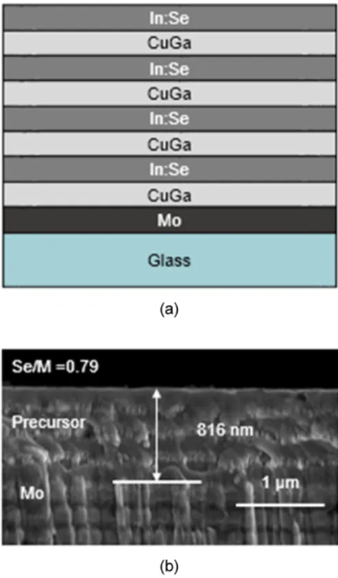
deposition of precursor and annealing of the precursor. Fig. 1(a) shows the schematic diagram of the precursor layer consisting of four alternative (In,Se)/(Cu,Ga) stacks, which was deposited by co-evaporation described in the experimental section.
The precursor layer was formed by repeated sequential co- evaporation of Cu+Ga and In+Se on a Mo-coated soda lime glass (SLG) at room temperature. The fluxes of Cu, In, Ga, and Se were maintained at 1.0, 1.9, 0.8, and 25 Å/s, respectively, as determined by a quartz crystal microbalance. After the deposition the precursor layer was somewhat intermixed as revealed from the Fig.1(b). The brighter line and darker line represent (Cu,Ga) layer and (In,Se) layer respectively. A precursor with four stacks of (In,Se)/(Cu,Ga) was selected because the metal precursor employed for precious development in Avancis Korea consisted of In/(Cu,Ga) four stacks. We wanted to minimize the experi- mental variation.
The overall cation composition in the precursor was main- tained with Cu/(In+Ga) = 0.8, Ga/(Ga+In) = 0.3, and Se/M = 0.79 (44% atomic Se among all). With the Cu composition of Cu/(In+Ga) = 0.8 the stoichiometric Se/M ratio in is 1.06. Our precursor with Se/M = 0.79 is in selenium-poor composition compared to the stoichiometric value.
The precursors were annealed in a Se environment for 30 min. However, the direct annealing of the precursor in a Se environment did not provide large grains and showed unwanted demarcation between stacked layers. Therefore, we introduced a pre-annealing in vacuum before the Se annealing. The sample
was naturally cooled down to 350°C in a Se environment and cooled down further in a vacuum.
2.2 Film characterization
The crystal structure of the annealed precursors and CIGS films was investigated using X-ray diffraction (XRD; RIKAKU Ultima IV x-ray diffractometer operated at 40 kV/40 mA with CuK
α11.405 Å) and Raman spectroscopy (LabRAM High Resolution Visible-NIR) with laser excitation wavelength of 532 nm. The morphologies of the films were analyzed using a scanning electron microscope (SEM, Nova230). The average composition of the precursor was analyzed using an energy dispersive spectroscopy (EDS) installed in the SEM. The atomic depth profile of the CIGS film was obtained by a time of flight secondary ion mass spectrometry (TOF-SIMS system from ION-TOF GmbH).
2.3 Cell fabrication
CIGS thin film solar cell devices were fabricated in an Al/ZnO:Al/i-ZnO/CdS/CIGS/Mo configuration structure. A 50-nm thick CdS buffer layer was deposited by chemical bath deposition using CdSO
4as a Cd source, thiourea as a sulfur source, and NH
3as a complexing agent. A transparent conductive
(a)
(b)
Fig. 1. Schematic cross-sectional diagram (a) and SEM cross- sectional image (b) of precursor consisting of four (In,Se)/
(Cu,Ga) stacks
oxide layer consisting of a 50-nm thick intrinsic ZnO layer and a 350-nm thick Al-doped ZnO layer was deposited by RF magnetron sputtering. The Al metal electrode was deposited by thermal evaporation through an aperture mask. The cell area (0.45 cm
2) is defined with mechanical isolation. The illuminated current-voltage (J-V) properties of the CIGS solar cells were measured using a solar simulator at an AM 1.5 spectrum illumination with 100 mW/cm
2intensity after calibration with a reference silicon solar cell.
3. Results and discussion
3.1 Direct annealing in Se environment
Fig. 2 shows the SEM cross-sectional images of CIGS film prepared by annealing in a Se environment at 450 and 550°C.
Four layers and the demarcation of four (In,Se)/(Cu,Ga) stacks are clearly seen by the direct selenization. Large grains are observed on the surface layer and all the other layers contains small grains corresponding to the thickness of each layer. Also the surface is very rough with many crevices. The direct growth of CIGS film is not successful from the morphology point of view. We need to devise a new way to improve the surface roughness and reduce crevices.
3.2 Phase evolution in vacuum annealing
The precursor was annealed in vacuum to enhance the chemical reaction from precursor to CIGS and analyzed the
phase formation at various temperatures.
Fig. 3 shows the SEM cross-sectional images of the CIGS films annealed at (a) 350°C, (b) 400°C, (c) 450°C, and (d) 500°C for 10 min in vacuum. The stacked-layer demarcation shown in the precursor disappeared at 350°C and compounds including CIGS and In
4Se
3were formed. At 400°C, round- shaped grains were formed and the grain sizes were about 250 nm. At 450°C, the film showed a dense film with increased grains sizes. A further increase in temperature 500°C the film showed a dense morphology with 1- μm size grains.
It is noted that no void was observed at the CIGS/Mo interface for the films annealed at 450 and 500°C. This suggests that annealing temperatures of 450 to 500°C are sufficient for growing large grains. However, the film consists of secondary phases as revealed by XRD studies, indicating that films must be annealed in selenium atmosphere to convert there remaining second phases into CIGS phase with large grain sizes for device applications. Based on the above experiments the precursors annealed at 400 and 450°C in vacuum were chosen as pre-annealing condition to obtain CIGS films.
Fig. 2. SEM cross-sectional images of CIGS film prepared by annealing in a Se environment at 450 and 550°C
Fig. 3. SEM cross-sectional images of CIGS films annealed at various temperatures in vacuum for 10 min
Fig. 4 shows the x-ray diffraction patterns of the precursors annealed in vacuum for 10 min. The precursors annealed at 300°C consist of In
2Se
3and Cu
2-xSe and Cu
4Ga
9phases, the 2θ peak position at 43.7° appears from Cu
2-xSe and Cu
9Ga
4. It clearly suggests that the (In,Se)/(Cu,Ga) stacks in the precursor were intermixed at these temperatures to form binary phases. As the temperature increased to 350°C the precursors had an intermetallic Cu
9(In,Ga)
4compound along with CIGS phase.
The peak of Cu
9Ga
4shifted to lower diffraction angles from 43.7 to 43° due to incorporation of In into Cu
9Ga
4phase.
As the temperature increased to 400°C the film showed Cu
9(In,Ga)
4,InSe, CIGS phases and another binary In
4Se
3compound. The CIGS phase was formed at this temperature due to reaction of In
4Se
3and Cu
4(In,Ga)
9phases. This is in agreement with the reported phases in the Cu-In-Ga system and the reaction mechanism from Cu-In-Ga precursors with selenium
6,15-17).
With further increase in temperature to 450 and 500°C the films contain CIGS and Cu
9(In,Ga)
4phases. Since the precursors were Se poor Se/M ratio =0.79, the precursors annealed in vacuum are not converted into CIGS films completely due to selenium re-evaporation from the precursor at 450 to 500°C which leads to formation of ternary metallic compounds. This
suggests that the selenium in the precursor is not sufficient for complete conversion into CIGS films indicating the requirement of external selenium flux during the film formation.
3.3 Phases after vacuum pre-annealing and Se annealing
Fig. 5 shows the Raman spectra of the CIGS films after pre-annealing in vacuum for 10 min and annealed in a Se environment for 30 min at 300, 400, and 500°C. In Raman spectroscopy the Cu
2-xSe binary phase can be well detected because of its high structural sensitivity compared to quaternary CIGS structure.
A Cu
2-xSe second phase existed after 300°C, which is also seen in the vacuum annealing. It means the Cu
2-xSe is originated by the reaction of Cu in (Cu,Ga) layer and Se in (In,Se) layer.
The Cu
2-xSe second phase completely disappeared at 400°C annealing and the InSe phase which was distinctly observed in vacuum annealing disappeared after Se annealing. Only pure Cu(In,Ga)Se
2phase is detected after Se annealing at 400 and 500°C, indicating that a complete CIGS phase is possible by Se annealing down to 400°C.
Fig. 6 shows the SEM cross-sectional images of CIGS films obtained by pre-annealing in vacuum for 10 min and then annealing in a Se environment for 30 min, named as two-step annealing. The film prepared at 400°C pre-annealing and 400°C Se annealing (V400+Se400) shows small grains with multi- layer structure. The demarcation of stacked precursor was pronouncedly revealed when the Se annealing temperature increased to 450°C as shown in Fig. 6(b). This suggests that 400°C pre-annealing is not high enough for large grains. It is necessary to increase the pre-annealing temperature higher than 400°C.
Fig. 4. XRD patterns of CIGS film annealed at various tem- peratures for 10 min in vacuum: 1 Cu2-xSe, 2 In2Se3, 3 Cu4(In,Ga), 4 CIGS, 5 In4Se3, 6 InSe, 7 Cu9(In,Ga)4
Fig. 5. Raman spectra of CIGS films annealed in vacuum for 10 min and then annealed in Se environment for 30 min at 300, 400, and 500°C
With pre-annealing 450°C and Se annealing at 450°C (V450+
Se450 in Fig. 6(c)) the outline of grains is more clearly seen and the demarcation of precursor stack layer was weakened compared to that of V400+Se450, suggesting that the CIGS was grown across the demarcation at 450°C in vacuum annealing.
Especially, the film grown by 450°C vacuum and 550°C Se annealing (marked as V450+Se550) revealed that the grains on the top side of the film were well aligned as bamboos and were densely packed each other with no grove at the grain boundaries.
Also the films also showed much less void in the film and on the bottom side of the film. The microstructure process with V450+
Se550 is a very desirable morphology with a smooth surface, well aligned grains on surface, and densely packed grains in the bulk, little voids at the bottom side of film, and no void at the CIGS/Mo interface.
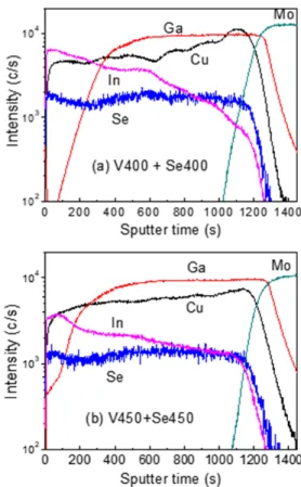
Fig. 7 shows the SIMS profile of Cu, In, Ga, and Se elements in the CIGS films pre-annealed in vacuum for 10 min and annealed in Se environment for 30 min at (a) 400°C (marked as
V400+Se400) and (b) 450°C (marked as V450+Se450).The film grown at 400°C as shown in Fig.7(a) shows the Ga concentration is sharply depleted at the CIGS surface and is uniform through the bottom side of CIGS film. The In con- centration is high at the surface and low at the bottom side of CIGS film. The Se concentration is homogenously distributed through the film depth. The Cu concentration is unevenly distributed through the film depth and accumulated at the Mo/CIGS interface.
The 400°C annealing led to the sharp depletion of Ga concentration at the surface and uneven distribution of Cu concentration within CIGS film. The Cu concentration is continuously and evenly distributed and the Ga at the surface is less depleted by annealing at 450°C as shown in Fig. 7(b).
The depletion of Ga at the surface is widely observed the CIGS films grown from two-step process, regardless of the nature of precursor stacks such as sputtered (Cu,Ga)/In
3), (Cu,In)/(Cu,Ga)
6), electroplated
9), oxide based precursors
10), Se containing precursor
11). The accumulation In and depletion of Ga at the surface are attributed to the preferential reaction of In with Se due to the difference in the electro negativity of In and Ga
6).
Fig. 6. SEM cross-sectional images of CIGS films pre-annealed in vacuum for 10 min and annealed Se environment for 30 min at various temperatures: (a) V400+Se400, (b) V400+Se450 (c) V450+Se450, and (d) V450+Se550
Fig. 7. SIMS depth profile of Cu, Ga, In, and Se in CIGS films pre-annealed in vacuum for 10 min and annealed in Se environment for 30 min at400(a) and 450oC (b)
Fig. 8 shows the depth profiles of Ga/(Ga+In) ratio in the CIGS films, determined from the calibrated SIMS profiles with reference to EDAX data. The film annealed at 400°C shows a Ga depletion down to 350-nm depth and a steep slope above 600-nm depth of CIGS film, increasing from 0.3 to 0.7. The film annealed at 450°C shows a Ga depletion down to 300-nm depth and a slow grade, increasing from 0.3 to 0.4.
The solid line in Fig. 8 is a reference GGI profile to obtain above 18% cell efficiency. The film we prepared has low GGI at the CIGS surface while Ga grading in the bulk can be adjusted by increasing the Ga composition in the precursor and with a more precise temperature control. However, the very low GGI at the CIGS surface is a big disadvantage, causing a low open- circuit voltage (V
oc).
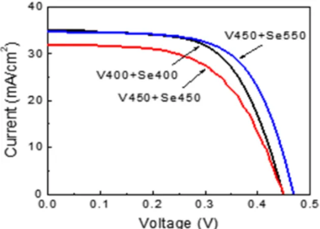
3.4 Cell performance
Fig. 9 shows the illuminated current-voltage curves of the CIGS solar cells fabricated with CIGS films grown at three different conditions. The photovoltaic parameters such as cell efficiency ( η), short-circuit current (J
sc), open-circuit voltage (V
oc), fill factor (FF), series resistance (R
s), and shunt resistance (R
sh) are listed in Table 1. The cell efficiency prepared with the CIGS film processed at 400°C (marked as V400+Se400 in Fig.
8) was 9.7%. The efficiency decreased to 8.3% as the annealing temperature increased to 450°C, marked as V450+Se450 in Fig.
9, due to smaller Jsc than the cell with 400°C-processed CIGS film. The reason of smaller J
scat 450°C is due to less grading of Ga depth profile in Fig. 8.
The efficiency again increased 10.4% when the CIGS film was pre-annealed at 450°C in vacuum and annealed at 550C in Se, marked as V450+Se550 in Fig. 9, due to the recovery of J
scand increase of both V
ocand FF. The improved conversion efficiency with 550°C Se annealing is attributed with improved surface roughness of the CIGS films.
The R
sand R
shfor CIGS film processed by V450+Se450 are 1.2 and 820 Ω ․ cm
2, respectively, and those for CIGS film processed by V450+Se550 are 0.7 and 1200 Ω ․ cm
2, respectively.
The typical R
shvalue of CIGS cells with a rough CIGS surface was in the range of 150~350 Ω ․ cm
2. The R
shvalue suggests that the CdS buffer could be covered more uniformly on the smooth CIGS surface, resulting in the sturdier buffer to reduce tunneling recombination through the CdS buffer layer. It is noted that the decrease of R
sand increase of R
shafter 550°C Se annealing resulted in the increase of both V
ocand FF.
In overall the V
ocis still too small due to low band gaps at the surface of the CIGS films, expected from Ga deficiency as shown in Fig. 8. To increase the band gap at the CIGS surface we need an additional vacuum post-annealing process to push Ga out to the surface. For the purpose, annealing above 550°C and short annealing time of 10 min are required to obtain better Ga homogeneity in the films
18,19). This is beyond the scope of this paper. Our paper reports a new a way to obtain a CIGS film with
Fig. 8. Depth profiles of Ga/(Ga+In) ratio in CIGS films annealedin vacuum for 10 min and in Se environment for 30 min at 400 (marked as V400+Se400) and 450°C (marked as V450+Se450)
Fig. 9. Illuminated current-voltage curves of CIGS thin film solar cells fabricated with three different CIGS films pre- annealed in vacuum for 10 min and annealed in Se environment for 30 min
Table 1. Photovoltaic parameters of CIGS solar cells fabricated with the CIGS films annealed at various conditions described in Fig. 8
Process η (%) Jsc
(mA/cm2) Voc
(V) FF
(%) Rs
(Ω·cm2) Rsh
(Ω·cm2) V400+
Se400 9.7 34.9 0.448 62 1.0 840
V450+
Se450 8.3 32.0 0.450 58 1.2 820
V450+
Se550 10.4 34.7 0.468 64 0.7 1200
a smooth surface, well aligned-grain on surface, densely- packed grains in the bulk, little voids in the bottom and at the CIGS/Mo interface.
4. Conclusions
CIGS absorbers were grown by a two-step process. A Se- containing precursor that consisted of four stacks of (In,Se)/
(Cu,Ga) layer was prepared by co-evaporation process. Growth of CIGS film by direct Se annealing was unsuccessful because the film showed small grains with clear demarcation between each stack. We introduced vacuum pre-annealing process before Se annealing to improve the film morphology.
The films grown at 450 and 500°C in vacuum showed a densely packed grains with large gains and little voids. The reason of densely packed grains was due to the formation of inter metallic phase during pre-annealing in vacuum. The precursor annealed at 300°C in vacuum had Cu
2-xSe and In
2Se
3phases. An InSe phase appeared at 400 and 450°C, and a ternary metallic Cu
9(In,Ga)
4appeared at 500°C.
The CIGS films obtained with 450°C pre-annealing and 550°C Se annealing a densely-packed CIGS film with a smooth surface, a well-aligned bamboo-like grains on top of the film, little voids in the bottom and at Mo/CIGS interface. The SIMS profile shows the Ga was depleted at the CIGS surface.
The film prepared with 450°C pre-annealing in vacuum and 550°C Se annealing that has the best morphology showed best cell performance 10.4% because of the smooth surface with well-aligned grains. The next step is to increase the band gap of the CIGS surface by alkaline post-deposition treatment and it is beyond the scope of this paper.
Acknowledgments
This work was financially supported by the Technology Development Program to solve climate changes from the National Research Foundation (NRF) of Korea (2016M1A2 A2936757) and by the Korea Institute of Energy Technology Evaluation and Planning (KETEP) (No. 20163030013690).
References
1. P. Jackson, R. Wuerz, D. Hariskos, E. Lotter, W. Witte, M.
Powalla, Effects of heavy alkali elements in Cu(In,Ga)Se2 solar cells with efficiencies up to 22.6%, Phys. Status Solidi, RRL, 10
583-586, 2016.
2. J. L. Wu, Y. Hirai, T. Kato, H. Sugimoto, V. Bermudez, “New world record efficiency up to 22.9% for Cu(In,Ga)(Se,S)2 thin film solar cell”, 7th World Conference on Photovoltaic Energy Conversion (WCPEC-7), Waikoloa, Hawaii, USA, June 10-15, 2018.
3. B. M. Basol, V. K. Kapur, A. Halani, C. R. Leidholm, H. Ullal, Cu(In,Ga)Se2 thin films and solar cells prepared by seleniza- tion of metallic precursors, J. Vac. Sci. Technol. A, 14, 2251-2256, 1996.
4. K. Kushiya, Y. Tanaka, H. Hakuma, Y. Goushi, S. Kijima, T.
Aramoto, Y. Fujiwara, Interface control to enhance the fill fac- tor over 0.70 in a large-area CIS-based thin-film PV technology, Thin Solid Films, 517, 2108-2110, 2008.
5. S. Y. Hsiao, P. C. Yang, H. C. Ni, K. Y. Yen, C. H. Chiu, P. S.
Lin, J. R. Gong, Characteristics of Cu(In,Ga)Se2 films pre- pared by atmospheric pressure Selenization of Cu-In-Ga pre- cursors using di-tert-butylselenide as Se source, J. Electrochem.
Soc., 159, H378–H383, 2012.
6. M. S. Kim, R. B. V. Chalapathy, K. H. Yoon, B. T. Ahn, Grain growth enhancement and Ga distribution of Cu(In,Ga)Se2 film using Cu2Se layer on Cu-In-Ga metal precursor, J. Electrochem.
Soc., 157, B154-B158, 2010.
7. W. Witte, D. Abou‐Ras, K. Albe, G. H. Bauer, M. Powalla, Gallium gradients in Cu(In,Ga)Se2 thin‐film solar cells, Prog.
Photovolt:Res. Appl., 23, 717-733, 2015.
8. R.Caballero, C.Maffiotte, C.Guillén, Preparation and charac- terization of Cu(In,Ga)Se2 thin films obtained by sequential evaporations and different selenization processes, Thin Solid Films, 474, 70-76, 2005.
9. M. Acciarri, S. Binetti, A. Le Donne, B. Lorenzi, L. Caccamo, L. Miglio, R. Moneta, S. Marchionna, M. Meschia, Development of a hybrid sputtering/evaporation process for Cu(In,Ga)Se2 thin film solar cells, ISO for Crystal Research Technology, 46, 871-876, 2011.
10. J. H. Shi, Z. Q. Li, D. W. Zhang, Q. Q. Liu, Z Sun, S. M.
Huang, Fabrication of Cu(In, Ga)Se2 thin films by sputtering from a single quaternary chalcogenide target, Prog. Photovolt:
Res. Appl., 19, 160–164, 2011.
11. M. Zhao, D. Zhuang, J. Han, Z. Gao, L. Guo, X. Li, R. Sun, M.
Cao, Annealing treatment of Cu(In,Ga)Se2 absorbers prepared by sputtering a quaternary target for 13.5% conversion effi- ciency device, Sol. Energy, 118, 375-383, 2015.
12. L. Zhang,D. Zhuang,M. Zhao,Q. Gong,L. Guo,L. Ouyang,R.
Sun, Y. Wei, S. Zhan, The effects of annealing temperature on CIGS solar cells by sputtering from quaternary target with Se-free post annealing, Appl. Surf. Sci., 413, 175-180, 2017.
13. M. Behr, M. Sharma, S. Sprague, N. Shinkel, J. Kerbleski, C.
Alvey, S. Rozeveld, T. Hasan, C. Wintland, M. Mushrush, A.Wall, Effect of growth conditions on microstructure of sput- tered precursor for CuIn1-xGaxSe2 (CIGS) absorber layer de- posited on stainless steel substrates, Thin Solid Films, 665, 36-45, 2018.
14. J. Koo, S. Jeon, M. Oh, H. I. Cho, C. Son, W. K. Kim, Optimization of Se layer thickness in Mo/CuGa/In/Se pre- cursor for the formation of Cu(In,Ga)Se2 by rapid thermal an- nealing, Thin Solid Films, 535, 148–153, pp. 2013.
15. M. Purwins, R. Enderle, M. Schmid, P. Berwian, G. Müller, F.
Hergert, S. Jost, R. Hock, Phase relations in the ternary Cu–Ga –In system, Thin Solid Films, 515, 5895–5898, 2007.
16. F. Hergert, R. Hock, A. Weber, M. Purwins, J. Palm, V. Probst.
In situ investigation of the formation of Cu(In,Ga)Se2 from se- lenized metallic precursors by x-ray diffraction—The impact of Gallium, Sodium and Selenium excess, J. Phys. Chem. Solids, 66, 1903–1907, 2005.
17. G. M. Hanket, W. N. Shafarman, B. E. McCandless, R. W.
Birkmire, Incongruent reaction of Cu–(In,Ga) intermetallic precursors in H2Se and H2S, J. Appl. Phys., 102, 74922, 2007.
18. K. Kim, H. Park, G. M. Hankert, W. K. Kim, W. N.
Shafarman, Composition and bandgap control in Cu(In,Ga)Se2 based absorbers formed by reaction of metal precursors, Prog.
Photovolt: Res Appl., 23, 765-772, 2014.
19. J. Koo, S. Kwon, Y. S. Roh, S. J. Lee, K. Y. Jung, W. N.
Shafarman, J. H. Park, D. H. Kim, J. M. Myoung, W. K. Kim, Effect of reaction temperature and time during two-step seleni- zation and sulfurization of Se-coated CuGa/In precursors, Electron. Mater. Lett., 12, 484-493, 2016.