Current Photovoltaic Research 4(2) 64-67 (2016) pISSN 2288-3274
DOI:http://dx.doi.org/10.21218/CPR.2016.4.2.064 eISSN 2508-125X
Ag 나노입자와 나노홀 배열구조를 이용한 초박형 단결정 Si 태양전지의 광흡수 증진
김수정ㆍ조윤애ㆍ손아름ㆍ김동욱*
이화여자대학교 물리학과, 서울특별시, 03760
Optical Absorption Enhancement for Ultrathin c-Si Solar Cells using Ag Nanoparticle and Nano-hole Arrays
Sujung Kim ․ Yunae Cho ․ Ahrum Sohn ․ Dong-Wook Kim*
Department of Physics, Ewha Womans University, Seoul, 03760, Korea
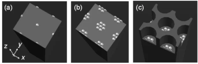
ABSTRACT: We investigated the influences of Ag nanoparticle (NP) arrays and surface nanohole (NH) patterns on the optical characteristics of 10- μm-thick c-Si wafers using finite-difference time-domain (FDTD) simulations. In particular, we comparatively studied the plasmonic effects of both monomer arrays (MA) and heptamer arrays (HA) consisting of identical Ag NPs. HA improved the optical absorption of the c-Si wafers in much wider wavelength range than MA, with the help of hybridized plasmon modes. The light trapping capability of the NH array pattern is superior to that of the Ag plasmonic NPs. We also found that the addition of the Ag HA on the wafers with surface NH patterns further enhanced optical absorption: the expected short-circuit current density was as high as 34.96 mA/cm
2.
Key words: Light trapping, Ultrathin c-Si, Plasmonic nanoparticle, Nanohole
Received April 26, 2016; Revised May 13, 2016;
Accepted May 16, 2016
ⓒ 2016 by Korea Photovoltaic Society
This is an Open Access article distributed under the terms of the Creative Commons Attribution Non-Commercial License (http://creativecommons.org/licenses/by-nc/3.0)
which permits unrestricted non-commercial use, distribution, and reproduction in any medium, provided the original work is properly cited.
Nomenclature
J
sc : short-circuit current density, mA/cm
2
Subscript
ARC : antireflection coating NP : nanoparticle
NH : nanohole
FDTD : finite-difference time-domain MA : monomer array
HA : heptamer array
LSPR : localized surface plasmon resonance
1. 서 론
결정질 실리콘 기반 태양전지는 높은 효율, 가격 경쟁력, 안정 성, 그리고 오랜 동안의 축적된 기술 등의 장점으로 다양한 태양 전지 소재 중에서도 독보적 우위를 누리고 있다. 태양광 발전 시 장에서의 더욱 확고한 경쟁력 확보를 위한 노력으로, 최근 50 μm 이하의 초박형 소자 개발에 대한 연구가 활발히 이루어지고 있 다
1-4). 또한, 초박형 실리콘 기판을 이용하면 유연하며(flexible) 착용 가능한(wearable) 소자 구현이 가능해지기 때문에 태양전 지 외에도 다양한 광전자 소자 활용이 가능할 것으로 기대된다
4). 기존 기판보다 훨씬 얇은 두께의 기판을 다루기 위해서는 공정 상의 이슈들도 많이 있겠지만, 충분한 광흡수를 얻는 것이 근원 적 난관에 해당하는 것으로 보인다. 특히, 실리콘은 간접천이형 (indirect bandgap) 반도체여서 광흡수계수가 다른 반도체 소재 보다 작기 때문에 효과적 광포획(light trapping) 기술 적용이 더 욱 절실하다.
기존 단결정 실리콘 태양전지에 쓰이는 광포획 기술에는 유 전체 박막의 상쇄 간섭을 이용하는 ARC, 다중반사를 위한 표면 텍스처링(texturing) 등의 방법이 있다. 또한, 광공명(optical
64