1. Introduction
Pipelining is a common paradigm for very high-speed digital system. A pipelining provides high speed because it allows many operations to be executed in parallel. But, in a conventional pipelining, the maximum operating frequency is limited by the slowest stage that has the longest
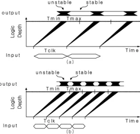
delay. Fig. 1-(a) shows logic depth timing diagram of conventional pipelining.
Wave pipelining is an alternative synchronous circuit clocking technique that allows overlapped execution of multiple operations without using synchronous elements within the logic. Data can be applied at a fastest rate than the delay of the logic block, the problem of clock distributionand clock skew is minimized. Fig. 1-(b) shows logic depth timing diagram of wave pipelining. The decision of maximum operating frequency in wave pipeline is difference between the slowest arriving signal and the fastest arriving signal. A high-speed and efficient implementation of wave pipelining requires
CMOS Clockless Wave Pipelined Adder Using Edge-Sensing Completion Detection
에지완료 검출을 이용한 클럭이 없는 CMOS 웨이브파이프 라인 덧셈기 설계
Yong-Sung Ahn
*, Jin-Ku Kang
*安 龍 城
*, 姜 晋 球
*Abstract
In this paper, an 8bit wave pipelined adder using the static CMOS plus Edge-Sensing Completion Detection Logic is presented. The clockless wave-pipelining algorithm was implemented in the circuit design. The Edge-Sensing Completion Detection (ESCD) in the algorithm is consisted of edge-sensing circuits and latches. Using the algorithm, skewed data at the output of 8bit adder could be aligned. Simulation results show that the adder operates at 1GHz in 0.35㎛ CMOS technology with 3.3V supply voltage.
요 약
본 논문은 CMOS 에지 완료검출 신호를 이용하여 8bit 웨이브파이프라인 덧셈기를 설게하였다. 이 구조는 클럭 이 필요 없이 동작한다. 에지감지후 신호완료를 검출하는 알고리즘회로는 센서회로와 래치로 구성되어있다. 제안 하는 구조를 이용하여 8bit 덧셈기의 출력이 거의 같은 시간에 만들어 지도록 정렬된다. 시뮬레이션에서 0.35um CMOS 공정을 사용하여 3.3V 공급전압으로 1GHz 동작을 확인하였다.
key words: CMOS, Clockless, wave-pipelined, Edge-sensing Completion detection
* 仁荷大學校 電子工學科
(Dept. of Electronic Eng., InHa Univ.)
接受日:2004年 2月 10日, 修正完了日:2004年 12月 10日
matched delay through all the propagation paths of the circuit.
In this paper, we introducea new clockless wave-pipelining approach. The proposed system eliminates intentional skew in the conventional wave pipelining. And, the clockless wave pipelining scheme with Edge-Sensing Completion Detection (ESCD) and propose an 8bit adder design which uses this technique.
( b ) Logic Depth
T im e I n p u t
o u t p u t
T c lk
T m in T m a x u n s t a b le s t a b le Logic Depth
T im e
I n p u t T c lk
T m in T m a x u n s t a b le s t a b le
( a ) o u t p u t
Fig. 1. (a) Conventional Pipelining(b) Wave Pipelining
그림1. (a) 기존의 파이프라이닝 구조 (b)웨이브파이프라인 구조
2. Wave pipelining approach
Wave pipelining is to remove internal registers from pipelining, including decreased latency as well as reduced area and power consumption. In a wave pipelining every stage holds the data for a short time, while the next stage starts to calculate the outputs to the stage after that. Wavepipelining decides operating frequency by difference between latest and earliest arriving signal. However, increasing the operating frequency requires fine intentional skew. Timing constraint space diagram is shown in Fig. 2.
Tmax Tmax 2 Tmin Tmin
2 Tmax
3
k=3 k=2
k=1
k=0
△
Tclk Tmax
Tmax
△ = Tclk
k : degree of wave-pipelining
△ : Intentional skew Tclk : clock period
Fig. 2. Timing constraint space diagram 그림. 2 타이밍 제약 공간 다이어그램
3. Proposed clockless wave-pipelining approach
Conventional wave pipelining require fine delayed clock signal for operation at high speed. But, it's hard to make fine delay for wave pipelining. We abandon clock signal to use. Our approach is based on asynchronous operation. This approach requires new circuit elements to detect the completion of computation in a logic block, but does not require the handshaking signals required by the conventional self-timed pipelining approach. The Edge-Sensing Completion Detection (ESCD) generates a pulse from the skewed output signals in combinational logic block. This pulse is used to latch the output signals for further processing. A block diagram of the ESCD is shown in Fig. 3. The ESCD consisted of edge-sensing circuits.
Edge-sensing circuits detecttransition of the outputs.
Where signals have transitions, the latest arriving signal is determined by ORing outputs from combinational block. ESCD aligns all signals to the latest arriving signal transition. The pulse is used
for pipelining latches.
Combinational circuit
L A T C H Edge-Sensing
Completion Detector
Input Data
Skewed Data
Output Data
Fig. 3. Block diagram of ESCD and latches 그림. 3 ECSD와 래치가 포함된 블록도
4. Edge-sensing completion detection circuit
The latest arriving signal detection process from tr ansition of outputs is as follows. Where a signal ha s transition, Edge-Sensing Circuit (ESC) detectstran sition of signal and generates a pulse. The latest ar riving signal is determined by ORing generated puls es. ESC is consisted of differentiator using passive elements and absolute-value circuit. A block diagra m of edge-sensing circuit is shown in Fig. 4.
V D D
V S S V D D
G N D
G N D V D D
V D D
G N D
D in D o u t
V D D
V S S
V D D
V S S
D in D o u t
Fig. 4. Edge-sensing circuit 그림 4. 에지 검출회로
Differentiator uses the transient current flow characteristics of RC circuit. But, When the transition change high into low in differentiator, generated negative pulse. ESC needs absolute-value circuit to solve. Absolute-value circuit consisted of inverter and nor-gate. Inverter supplied voltage from VDD to GND amplifies detection signal of positive transition. And, inverter supplied voltage from VDD
to VSS amplifies detection signal of negative transition. The inverter controloperating point, change signal range VDD to GND. ORing detection signal of negative and positive transitions.
5. Clockless wave pipelining adder design
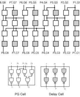
Our approach, using wave pipelining and ESCD technique is applied to an 8bit carry look-ahead adder (CLA) design. The CLA is selected because of its regularity to implementation of the pipelining design technique. Fig. 5 shows the block diagram of CLS designed based on our proposed ESCD algorithm. It consists of PG Generator, carry generator, and sum generator. In the PG generator, the propagation terms and generation terms are produced from XOR-gate and AND-gate. The propagate term and carry term are generated by providing those signals to the carry generator. At the final stage, the sum is produced. In order to reducethe propagation delay difference the padding elements were inserted in the carry generator.
PG Generator
Carry Generator
Sum Generator
Input A Input B
Skewed data
latched data Completion detection
&
Latch
Fig. 5. Block diagram of the CLA with proposed ESCD scheme
그림5. 제안한 ESCD구조를 사용한 CLA 블록도
Fig. 6 shows the block diagram of the Carry generator. Padding elements are used for balancing
the delay path between the longest and shortest paths. By reducing the delay difference the higher speed wave-pipelined system can be realized. In addition to that, in order to align the skews of sum values from the Sum generator, the proposed ECSD scheme was applied to the final sum generator block. Thus the final sum outputs have little skews.
P1,G1 P2,G2 P3,G3 P4,G4 P5,G5 P6,G6 P7,G7 P8,G8
P1,C1 P2,C2 P3,C3 P4,C4 P5,C5 P6,C6 P7,C7 P8,C8
f Pr Pl Gr Gl
f P G
f Pl Gl
f P G
Delay Cell PG Cell
Fig. 6. Block diagram of the Carry generator 그림6. Carry generator 블록도
The 8bit input data of A and B were provided in parallel and the skewed 8bit output signals of the sum and 1bit carry-out signal came from the CLA.
The skewed output data from the CLA due to the data dependency of the CMOS gates or propagation pathdelay difference were supplied to ESCD block.
A static CMOS circuit was used to simplify the design procedure and low power consumption. The circuit was designed using 0.35㎛ CMOS technology with 3.3V power supply. Fig. 7 shows the output signals from the ESCD to latch the signals in the pipelining stage. The figure shows that pulse signals were generated whenever there were transitions in the sum and carry-out from the CLA.
Otherwise a timing pulse signal was not generated.
The skewed data are to be latched by ESCD. Fig. 8 shows skewed data and latched data in the pipelining stage. As shown in the figure, the skew of about 300ps in the data output are reduced to almost zero after the latching. The 8bit input data were simulated at a rate of 1GHz.
Fig. 7. Simulated (a) output signals at pipelining latches and (b) generated from ESCD
그림7. 시뮬레이션파형 (a) 파이프라이닝래치에서의 출력신호
(b) ECSD에서부터 생성된 신호
Fig. 8. Simulated results of (a) skewed data and (b) aligned data
그림. 8. (a)정렬되기 전 출력 (b) 정렬된 출력
Compared to the results from ref.[12], the operating speed is improved to 1 GHz compared to 800MHz and the final skews are reduced to about zero compared to 70ps.
6. Conclusion
We design pipelined adder using wave pipelining methodology and ESCD. ESCD can be detecting the latest arriving signal in skewed data. Our approach uses 8bit wave pipelined adder for detecting completion. The variation of output latched by generated signal in ESCD. The adder has been operated at 1GHz in 0.35㎛ CMOS technology with 3.3V power supply.
Reference
[1]L.W. Cotton, "Maximum-rate pipelining systems,"
1969 AFIPS Proc. Spring Joint Computer Conf, Vol.34, Montvale, NJ: AFIPSPress, pp. 581-586, May 1969.
[2] I. Sutherland, "Micropipelines", Commun. ACM, pp. 720-738, 1989.
[3]C. T. Gray, W. Liu, and R. Cavin III, Wave Pipelining:
Theory and CMOS Implementation,
Kluwer Academic Publishers, Oct. 1993.[4]Wentai Liu, et al, "A 250MHz Wave pipelined Adder in 2㎛ CMOS" IEEE, Journal of solid-state
circuits.Vol.29, pp. 1117-1127, Sep. 1994.
[5]C. T. Gray, et al, "Timing Constraints for Wave-Pipelined Systems"
IEEE, Trans.
Computer-Aided Design,
Vol.13, NO. 8, pp.987-1004, Aug. 1994.
[6] A. S. Sedra, et al, "Microelectronic circuits"4th Ed, Oxford Univ. Press, pp. 1022-23, 1998.
[7]Wayne P. Burleson, et al, "Wave-Pipelining: A Tutorial and Research Survey" IEEE, Transactions
of VLSI Systems, Vol.6, NO. 3, pp. 464-474, Sep.
1998.
[8]D. C. Wong, et al, "Designing High-Performance Digital Circuits Using Wave Pipelining: Algorithms and Practical Experiences"
IEEE, Trans.
Computer-Aided Design, Vol.12, NO. 1, pp. 25-46,
Jan. 1993.[9]M.Singh, S. M. Nowick. "MOUSETRAP:
Ultra-High-Speed Transition-Signaling Asynchronous Pipelining" IEEE, ICCD 2001, pp.
9-17, 2001.
[10]Klass, E. F. "Wave Pipelining: Theoretical and Practical Issues in CMOS" Ph.D. Thesis, Technical University Delft, 1994.
[11]B. Lim, Jin-Ku Kang "A Self-Timed Wave Pipelined Adder Using Data Align Method" IEEE,
AP-ASIC 2000., pp. 77-80. Aug. 2000.
[12]Jin-Ku Kang "Self-timed pipelined using latest arriving signal detection" Electronics Letters, Vol.37, No.10, pp.615-617, May. 2001.
저 자 소 개
安 龍 城
2002년 인하대학교 전자. 전기 컴퓨터공학부 졸업
2004년 인하대학교 전자. 전기 컴퓨터공학부 석사졸업.
현재 (주)SiliconWorks 회로 설계팀
관심분야 : CMOS고속회로 설계, VLSI, 신호처리회로설계
姜 晋 球
1983 서울대학교 공학사.
1990 New Jersey Institute of Technology 전자공학 석사, 1996 North Carolina State University, 전자 및 컴퓨터공학 박사.
1983-1988 삼성반도체 1996-1997 미국 INTEL 선임설계연구원.
1997. 3월 - 현재 인하대학교 전자공학과 부교수
관심분야: 고속 CMOS회로설계. 혼합모드 회로설계, 통신용회로설계