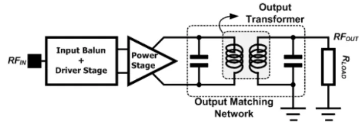
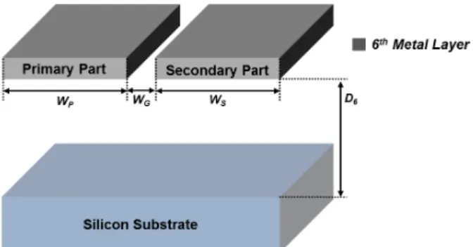
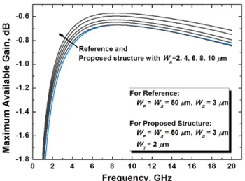
A Low-Loss On-Chip Transformer Using an Auxiliary Primary Part (APP) for CMOS Power Amplifier Applications
4
0
0
전체 글
(2)
(3)
(4)
수치
관련 문서
