• 검색 결과가 없습니다.

A Study on Electrical Characteristics and Optimization of Trench Power MOSFET for Industrial Motor Drive

N/A
N/A
Protected

Academic year: 2021

Share "A Study on Electrical Characteristics and Optimization of Trench Power MOSFET for Industrial Motor Drive"

Copied!
6
0
0

로드 중.... (전체 텍스트 보기)

전체 글

(1)

A Study on Electrical Characteristics and Optimization of Trench Power MOSFET for

Industrial Motor Drive

Ey Goo Kang

*

Abstract

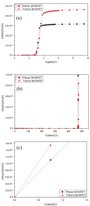
Power MOSFET is developed in power savings, high efficiency, small size, high reliability, fast switching, and low noise. Power MOSFET can be used in high-speed switching transistors devices. Recently attention given to the motor and the application of various technologies. Power MOSFET is a voltage-driven approach switching device and designed to handle on large power, power supplies, converters, motor controllers. In this paper, the 400 V Planar type, and the trench type for realization of low on-resistance are designed.

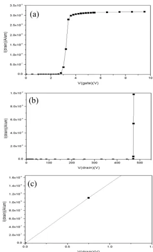
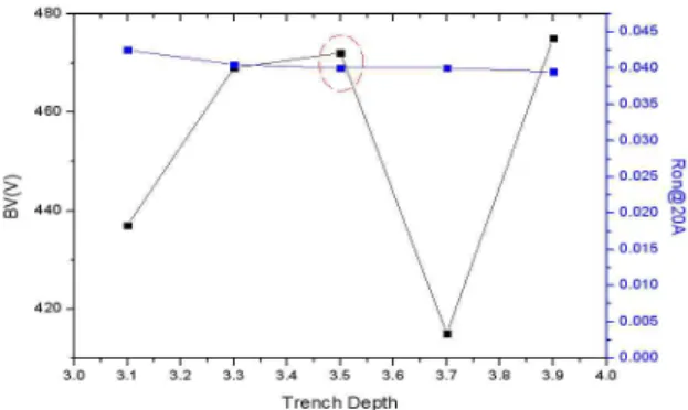
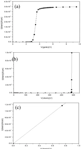
Trench Gate Power MOSFET Vth : 3.25 V BV : 484 V Ron : 0.0395 Ohm has been optimized.

Keywords: Power MOSFET, Planar process, Trench process, Breakdown voltage, On resistance, P-base dose

* Dept. of Photovoltaic Engineering, Far East University

Corresponding author:[email protected], Tel:+82-43-879-3590

Manuscript received Aug. 16, 2013; revised Sep.

15,2013 ; accepted Sep 16. 2013

1. Introduction

The power MOSFET, a device operated in a voltage drive method and a switching device designed to handle big power, is widely used in a power supply device, converter, motor controller, etc.

The Power MOSFET has low on-state resistance, so it can raise efficiency by reducing power transmission loss in an operating condition, eventually enabling low-power realization.[1-3] This study designed a 400V grade Planar Power MOSFET, designed and simulated a 400V

grade Trench type Power MOSFET based on this, and analyzed its breakdown voltage and on-state resistance characteristics through this.[4-5]

Ⅱ. Experiment Method

2.1 Design of a 400V Grade Planar Power MOSFET

Before designing a Trench Power MOSFET of 400V grade breakdown voltage, this study basically designed and optimized a planar

Fig. 1. The structure of 400V Planar Power MOSFET

power MOSFET of the same unit cell size as a

Trench Power MOSFET. This study designed a

basic Planar Power MOSFET structure of over 400V

(2)

grade through a simulation, whose final design structure and parameter value are shown in Fig.1 and Table 1 below. The simulation tool was used TCAD.

Table 1. The design and process parameters of 400 V Planar Power MOSFET Parameter

Parameter 400 V/20 A

Cell Pith 8.25 ㎛

Gate width 4.25 ㎛

N+ width 1 ㎛

Epi Depth 40 ㎛

P base Depth 3.25 ㎛

Wafer Depth 320 ㎛

Epi resistivity 9.75 Ωcm Wafer resistivity 0.018 Ωcm

P+ Source dose 3e15cm

-2

Energy 120 KeV P Base dose 4e13cm

-2

Energy 80 KeV N JFET dose 1E10cm

-2

Energy 100 KeV N+ Source dose 5E15cm

-2

Energy100 KeV

The operating characteristics of a 400V grade Planar Power MOSFET are shown in Fig.2 and Table 2 below.

2.2 Design of a 400 V Trench Power MOSFET

A trench gate was applied to an optimized 400V Planar Power MOSFET structure. A simulation was carried out, with Cell Pitch, Epi Depth, Wafer depth, Epi resistivity and Gate Width fixed. Fig.3 below shows a basic structure of Trench Power MOSFET.

(a)

(b)

(c)

Fig. 2. The electrical characteristics of optimal planar Power MOSFET. (a) Vth, (b) BV, (c) Ron.

Table 2. The electrical characteristics of optimal planar Power MOSFET.

Vth BV(V) Ron@20 A

3.1V 470V 0.056

Fig.3. The structure of 400 V Trench Power MOSFET

(3)

2.3 Breakdown voltage and on-state resistance simulation depending on trench gate depth

This paper gave a condition of gate depth as 3.1∼

3.9 um. The Trench Power MOSFET reduces the JFET area and drift area by etching the gate differently from the Planar Power MOSFET. It could be seen that this can reduce on-state resistance compared to the Planar Power MOSFET structure.

However, etching the gate too deep can reduce breakdown voltage due to the concentrated electric field on the increased part of gate etching depth without increasing the electric field uniformly, so the simulation was carried out by paying attention to this. This simulation was carried out with a criterion because 3.5 um was judged to be suitable.

Fig. 4. The breakdown voltage and on resistance of trench power MOSFET according to Trench depth

Table 3. The breakdown voltage and on resistance of trench power MOSFET according to Trench depth Trench

Depth(㎛) BV(V) Ron@20 A

3.1 437 0.0425

3.3 469 0.0405

3.5 472 0.04

3.7 415 0.04

3.9 475 0.0395

2.4 Threshold voltage and on-state resistance simulation depending on P-base dose

A condition of P-base dose 1.0E13∼3.0E13 cm

-2

was given, with the previous results fixed. If the

P-base dose increases, the gate voltage should be increased to form a channel, so the threshold voltage increases, but if the threshold voltage is high, the switching speed decreases, so it should be designed low. If the threshold voltage decreases, the switching time is improved, but undesired turn-on may happen due to the gate voltage raised during switching. In addition, the Trench Power MOSFET creases a channel beside the trench gate differently from the Planar Power MOSFET, so concentration was set differently to obtain the same threshold voltage. This paper assumed threshold voltage as 3.0∼4.0V, so 3.2V was obtained per 1.5E13 cm

-2

suitable for this condition and the on-state resistance was also low, therefore 1.5E13 cm

-2

was adopted.

Fig. 5. The threshold voltage and on resistance characteristics according to P-base dose

Table 4. The threshold voltage and on resistance characteristics according to P-base dose P Base

dose(cm

-2

) V

th

(V) Ron@20 A

1.0e13 2.56 0.0395

1.5e13 3.25 0.0395

2.0e13 4.0 0.04

2.5e13 4.71 0.04

3.0e13 5.43 0.0405

The comparison contents of Planar and Trench are

shown in Fig.6 and Table 5 respectively. It could be

seen that on-state resistance was reduced due to the

Trench gate.

(4)

Type V

th

(V) BV(V) Ron

@20 A

Planar 3.1 470 0.056

Trench 3.25 473 0.0395

(a)

(b)

(c)

Fig. 6. The electrical characteristics of optimal Planar and trench power MOSFETs (a) Vth, (b) BV, (c) Ron.

Table 5. The electrical characteristics of optimal Planar and trench power MOSFETs (a) Vth, (b) BV, (c) Ron.

2.5 Breakdown voltage on-state resistance simulation depending on cell pitch and gate area

The gate area was reduced to 8.25∼6.25 um depending on cell pitch and designed as 4.25∼2.25 um through reduction by 1 um in proportion to the cell pitch.

Fig. 7. The breakdown voltage and on resistance

characteristics of trench power MOSFET according to cell pitch, gate width

Table 6. The breakdown voltage and on resistance

characteristics of trench power MOSFET according to cell pitch, gate width

Cell

pitch(㎛) Gate

width(㎛) BV(V) Ron

@20 A

8.25 4.25 473 0.0395

7.25 3.25 479 0.0395

6.25 2.25 484 0.0395

As a result of simulation, it could be seen that it is possible to raise the efficiency per net die compared to the Planar Power MOSFET by reducing the device cell length of a Trench Power MOSFET.

Ⅲ. Result and Consideration

The final 400V grade Trench Power MOSFET

was simulated, whose optimized parameters and

characteristics are shown in Fig.8, 9 and Table 7 and

8 below.

(5)

(a)

(c)

Fig. 8. The electrical characteristics of optimal trench power MOSFET (a) Vth, (b) BV, (c) Ron.

Fig. 9. Trench Power MOSFET optimiation sectional view.

Table 7. The electrical characteristics of optimal trench power MOSFET

V

th

(V) BV(V) Ron@20 A

3.25 484 0.0395

Table 8. Optimal design and process parameter 400 V sized trench power MOSFET.

Parameter 400 V/20 A

Cell Pith 6.25 ㎛

Gate width 2.25 ㎛

Trench Depth 3.5 ㎛

N+ width 1 ㎛

Epi Depth 40 ㎛

P base Depth 3 ㎛

Wafer Depth 320 ㎛

Epi resistivity 9.75 Ωcm Wafer resistivity 0.018 Ωcm

P+ Source dose 3e15cm

-2

Energy 120 KeV P Base dose 1.5e13cm

-2

Energy 80 KeV N+ Source dose 5E15cm

-2

Energy100 KeV

Ⅳ. Conclusion

As a result of simulation, the Trench Power MOSFET can reduce on-state resistance of the trench gate part on the JFET area compared to the Planar Power MOSFET. Also, the efficiency could be raised by reducing power supply loss with low on-resistance by reducing the resistance in the drift area. In addition, by reducing the cell size, the Trench Power MOSFET can have higher efficiency than the Planar Power MOSFET and raise the breakdown because the number of net dies increases.

References

[1] Fujihira, T, Proc. of the ISPSD’98, Kyoto(1998), pp.423-426

[2] H. Ninomiya, Y.Miura and K Kobayashi, Proc. ISPSD(2004), pp.177-180

[3] Pravin N. Kondekar, TENCON Vol.4(2003),

(b)

(6)

pp.1455-1458.

[4] S. Iwamoto, K. Takahashi, H. Kuribayashi, S. Wakimoto, K. Mochizuki and H. Nakazawa, Power Semiconductor Devices and Ics, Proceedings.

ISPSD’05. The 17thInternationalSymposiumon(2005), pp.31-34

[5] Yoshiyuki Hattori, Kyoko Nakashima, Makoto Kuwahara, Tomoyuki Yoshida, Shoichi Yamauchi and Hitoshi Yamaguchi, Proceedings of International symposium on Power Semiconductor Devices & ICs, Kitakyushu(2004), pp.189-192

[6] E.G. Kang, S.H. Moon and M.Y. Sung, Microelectronics journal, Vol.32, Issue.8(2001), pp.641-647

[7] E.G. Kang and M.Y. Sung, Solid-State Electronics, Vol.46, Issue.2(2002), pp.295-300

BIOGRAPHY

EyGooKang (Life Member)

2000 : BS degree in Electrical Engineering, Korea University.

2005 : MS degree in Electrical Engineering, Korea University.

2006 : PhD degree in Electrical Engineering, Korea University.

2003~present : professor in

department of photo voltaic engineering, Far East

University

수치

Fig. 1. The structure of 400V Planar Power MOSFET
Table 1. The design and process parameters of 400 V Planar Power MOSFET Parameter
Table 3. The breakdown voltage and on resistance of trench power MOSFET according to Trench depth Trench Depth(㎛) BV(V) Ron@20 A 3.1 437 0.0425 3.3 469 0.0405 3.5 472 0.04 3.7 415 0.04 3.9 475 0.0395
Fig. 6. The electrical characteristics of optimal Planar and trench power MOSFETs (a) Vth, (b) BV, (c) Ron.
+2

참조

관련 문서