다양한 매칭 회로들을 활용한 저잡음 증폭기 설계 연구
853
다양한 매칭 회로들을 활용한 저잡음 증폭기 설계 연구
Design of Low Noise Amplifier Utilizing Input and Inter Stage Matching Circuits
Sung-Hun Jo
**Assistant professor, Department of Electronic Engineering, Dongseo University, Busan, 47011 South Korea
ABSTRACT
In this paper, a low noise amplifier having high gain and low noise by using input and inter stage matching circuits has been designed. A current-reused two-stage common-source topology is adopted, which can obtain high gain and low power consumption. Deterioration of noise characteristics according to the source inductive degeneration matching is compensated by adopting additional matching circuits. Moreover trade-offs among noise, gain, linearity, impedance matching, and power dissipation have been considered. In this design, 0.18-mm CMOS process is employed for the simulation. The simulated results show that the designed low noise amplifier can provide high power gain and low noise characteristics.
Keywords : Low noise amplifier, Matching circuit, Maximum gain, Minimum noise figure
Ⅰ. Introduction
Low noise amplifier (LNA) is a key building block in modern electrical system. LNA amplifies a very weak signal at the front end of the wireless receiver. The first stage in wireless receiver has the most significant effect on the noise performance of the entire system because the effect of noise from subsequent stages are reduced by
stage gains [1], [2]. Thus, the LNA locating at the first stage in wireless receiver is required to have minimum noise figure and maximum gain. Moreover, in designing the LNA, trade-offs among noise, gain, linearity, impedance matching, and power consumption should be considered [3], [4]. In particular, the main process of LNA design is to simultaneously perform input matching and noise matching under a given amount of power consumption. In this paper, a current-reused two-stage common-source LNA topology utilizing input stage, inter stage, and output stage matching circuits is designed, which can obtain high gain and low noise characteristics.
Ⅱ. Designed System Architecture
A simplified schematic of the cascode LNA topology is shown in Fig. 1 [5]. The miller effect can be eliminated in cascode structure, which improves isolation between input and output matching circuits [6]. That is, inverse leakage signal can be effectively suppressed. In addition, in order to reduce power consumption in the cascode structure, the size of the transistor M1 should be sufficiently small. That is, the gate-source capacitance (C
gs) of transistor M1 should be small, which requires a large value of L
S. However, when the value of L
Sis increased, minimum achieveble noise figure(NF) increases, which causes deterioration of noise characteristics. By adding C
ex, deterioration of noise characteristics can be prevented without increasing the size of the transistor M1. However, since the gain decreases as the value of C
exincreases, it is important to select C
exand L
Swith adequate values in consideration of performance trade-offs.
Received 27 April 2021, Revised 1 May 2021, Accepted 10 May 2021
* Corresponding Author Sung-Hun Jo(E-mail:[email protected], Tel:+82-51-320-4226)
Assistant professor, Department of Electronic Engineering, Dongseo University, Busan, 47011 South Korea
Open Access http://doi.org/10.6109/jkiice.2021.25.6.853
print ISSN: 2234-4772 online ISSN: 2288-4165Short Paper
한국정보통신학회논문지 Vol. 25 No. 6: 853~856, Jun. 2021
한국정보통신학회논문지 Vol. 25, No. 6: 853-856, Jun. 2021
854 Fig. 1 Simplified schematic of the cascode LNA
Fig. 2 Schematic of designed LNA
Moreover, adding C
exleads to a decrease in power consumption, which can deteriorate linearity. In order to improve the linearity, the value of transconductance of transistor M1 must be increased, but this means an increase in power consumption. Therefore, it becomes difficult to overcome the trade-off between linearity and current consumption in a design where the amount of usable power is limited. Thus, in a design requiring low power consumption, the current-reused method can be effectively used [3], [7]. By combining cascode and current-reused method, low power consumption and high gain can be obtained.
Designed current-reused two-stage common-source LNA topology is shown in Fig. 2. The designed topology can achieve high gain characteristic through low power consumption, but it has a disadvantage of deteriorating the noise figure. Thus, to prevent deterioration of the noise figure, an input matching circuit is utilized.
Fig. 3 Power gain of the designed LNA
Fig. 4 Noise figure of the designed LNA
Fig. 5 IIP3 of the designed LNA
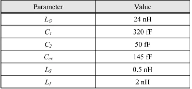
Table. 1 Design parameters
Parameter Value
L
G 24 nHC
1 320 fFC
2 50 fFC
ex 145 fFL
S 0.5 nHL
1 2 nH다양한 매칭 회로들을 활용한 저잡음 증폭기 설계 연구
855 Table. 2 Performance summary
Parameter Value
Target Frequency 2 GHz
NF 0.5 dB
S21 20.3 dB
S11 -17.4 dB
IIP3 -12.1 dBm
Power dissipation 5.3 mW
Supply voltage 1.8 V
CMOS Technology 0.18 mm
In the source inductive degeneration matching scheme, a relatively high bias current is required to achieve simultaneous power and noise matching. Therefore, if this scheme is used in a design that requires low power consumption, noise figure becomes worse. Thus, to prevent deterioration of the noise figure, an input matching scheme is also used. Previously, input matching was performed only through L
G, C
ex, and L
S. By adding C
1and C
2, input matching can be performed effectively even when low power consumption is required. That is, value of L
Scan be reduced to improve gain and noise figure while maintaining input matching through adjustment of L
G, C
1, and C
2values.
Furthermore, the two transistors M1 and M2 share the same bias current to reduce power consumption. The amplified signal from the transistor M1 is applied to the gate of the transistor M2 through the coupling capacitor C
4, and the capacitor C
3acts as a by-pass capacitor for the transistor M2. In the designed structure, L
G, C
1, C
2, C
ex, and L
Sare adopted for simultaneous power and noise matching. In addition, L
2and R
Dwere used for output matching, and an LC network (L
1-C
4) between the gain
stages was used for inter stage matching.
In order to obtain the minimum noise figure and maximum gain, the value of V
gsof transistor M1 must be determined. After that, the size of the transistor M1 is determined in consideration of the available power budget. As the size of the transistor M1 becomes smaller, power consumption decreases, but the cut-off frequency also decreases, thus it is important to determine an appropriate size of transistor M1. In this design, when V
gsis equal to about 600 mV, it shows the maximum gain and minimum noise characteristics.
Fig. 3 shows power gain (S21) of about 21.3 dB at 2 GHz. Noise figure (NF) of the designed LNA is shown in Fig. 4. It represents a value of about 0.5 dB at 2 GHz.
Third order input intercept point (IIP3) is shown in Fig.
5. The extrapolated lines intersect on about –12.1 dBm.
Moreover, design parameters are shown in the Table 1.
Various components including capacitors, inductors, and resistors are adopted to implemented the designed structure. Performance of designed LNA is summarized in the Table 2. It has been designed to target of the 2 GHz and implemented using 0.18-mm CMOS process.
Ⅲ. Conclusion
In this paper, LNA utilizing various matching circuits is designed. current-reused two-stage common-source topology is adopted, which can obtain a high gain through low power consumption. Deterioration of noise figure according to current-reused two-stage common- source topology and inductive source degeneration matching is compensated by utilizing additional matching circuits.
ACKNOWLEDGEMENT
This work was supported by the Dongseo University Research Fund of 2020. (DSU-20200028)
Parameter Value
L
2 10 nHR
D 900 ΩC
3 630 fFC
4 500 fFM1(W/L) 60 mm / 0.18 mm
M2(W/L) 60 mm / 0.18 mm
한국정보통신학회논문지 Vol. 25, No. 6: 853-856, Jun. 2021
856
REFERENCES
[ 1 ] H. Rashtian and S. Mirabbasi, “Applications of Body Biasing in Multistage CMOS Low-Noise Amplifiers,” IEEE
Transactions on Circuits and Systems I: Regular Papers,
vol. 61, no. 6, pp. 1638-1647, Jun. 2014.[ 2 ] M. El-Nozahi, E. Sanchez-Sinencio, and K. Entesari, “A Millimeter-Wave (23-32 GHz) Wideband BiCMOS Low- Noise Amplifier,” IEEE Journal of Solid-State Circuits, vol.
45, no. 2, pp. 289-299, Feb. 2010.
[ 3 ] M. Parvizi, K. Allidina, and M. N. El-Gamal, “An Ultra-Low-Power Wideband Inductorless CMOS LNA With Tunable Active Shunt-Feedback,” IEEE Transactions on
Microwave Theory and Techniques, vol. 64, no. 6, pp.
1843-1853, Jun. 2016.
[ 4 ] J. Hu, K. Ma, S. Mou, and F. Meng, “A Seven-Octave Broadband LNA MMIC Using Bandwidth Extension Techniques and Improved Active Load,” IEEE Transactions
on Circuits and Systems I: Regular Papers, vol. 65, no. 10,
pp. 3150-3161, Oct. 2018.[ 5 ] G. Girlando and G. Palmisano, “Noise figure and impedance matching in RF cascode amplifiers,” IEEE Transactions on
Circuits and Systems II: Analog and Digital Signal Processing, vol. 46, no. 11, pp. 1388-1396, Nov. 1999.
[ 6 ] P. Wei, M. Tsai, S. Hsu, C. Shen, and T. Wu, “An Electromagnetic Bandgap Structure Integrated With RF LNA Using Integrated Fan-Out Wafer-Level Package for Gigahertz Noise Suppression,” IEEE Transactions on
Microwave Theory and Techniques, vol. 66, no. 12, pp.
5482-5490, Dec. 2018.
[ 7 ] P. Qin and Q. Xue, “Design of Wideband LNA Employing Cascaded Complimentary Common Gate and Common Source Stages,” IEEE Microwave and Wireless Components