한국정보통신학회논문지 Vol. 24, No. 5: 682-685, May. 2020
682
C
gd성분을 포함한 공정별 주요 잡음원 천이 과정 연구
The transition of dominant noise source for different CMOS process with C gd
consideration
Minsuk Koo
**Ph. D student, Department of Electrical Engineering, Purdue University, West Lafayette, IN 47907, U.S.A
ABSTRACT
In this paper, we analyze the dominant noise source of conventional inductively degenerated common-source (CS) cascode low noise amplifier (LNA) when width and gate length of stacked transistors vary. Analytical MOSFET and its noise model are used to estimate the contributions of noise sources. All parameters are based on measured data of 60nm, 90nm and 130nm CMOS devices. Based on the noise analysis for different frequencies and device parameters including process nodes, the dominant noise source can be analyzed to optimize noise figure on the configuration. We verified analytically that the intuctively degenerated CS topology can not sustain its benefits in noise above a certain operation frequency of LNA over different process nodes.
Keywords : CMOS process, noise figure, low noise amplifier (LNA), noise transition point, Cgd consideration.
Ⅰ. Introduction
A low noise amplifier (LNA) is one of the most critical circuit block in a wireless transceiver. As the first block to interface the incoming RF signal from antenna, noise figure of LNA dominates overall noise performance
of the system. As the scaling down of CMOS technology continues, the most advanced short channel MOSFETs have achieved cutoff frequency (f
T) and maximum oscillation frequency (f
MAX) higher than 200 GHz [1-2].
Consequently, the operation frequency of CMOS circuits easily go up to several tens of gigahertz range. Although these indices suggest the feasibility of CMOS devices for the operation [3], they do not provide design insights for RF circuit optimization. To that affect, many researchers have explored the design optimization using device parameters in ahead of actual design [4-5]. Also, studies on different topologies of LNA for various frequency band with fixed process node have conducted [6-7]. However, little research results on dominant noise source analysis have been reported for different process node and design parameters.
In this paper, we analyze noise figure of LNA by dividing it into three components with analytical models.
For better estimation, we additionally considered following components that are usually not considered in conventional model but affect more at higher frequency:
gate to drain capacitance (C
gd), gate electrode resistance of transistor, parasitic resistance of inductors, and etc.
We present an approach to optimize the design of LNA with inductively degenerated common-source (CS) cascode configuration. The analysis on transition point of dominant noise sources for different process node gives us an insight on design parameters that we are supposed to focus on to improve noise performance.
Ⅱ. Noise figure of cascode LNAs with Cgd consideration
Conventional inductively degenerated CS cascode
Received 10 May 2020, Revised 11 May 2020, Accepted 13 May 2020
* Corresponding Author Minsuk Koo (E-mail: [email protected], Tel:+1-765-714-5135)
Ph. D student, Department of Electrical Engineering, Purdue University, West Lafayette, IN 47907, U.S.A
Open Access
http://doi.org/10.6109/jkiice.2020.24.5.682
print ISSN: 2234-4772 online ISSN: 2288-4165Short Paper
한국정보통신학회논문지 Vol. 24, No. 5: 682~685, May. 2020
Cgd 성분을 포함한 공정별 주요 잡음원 천이과정 연구
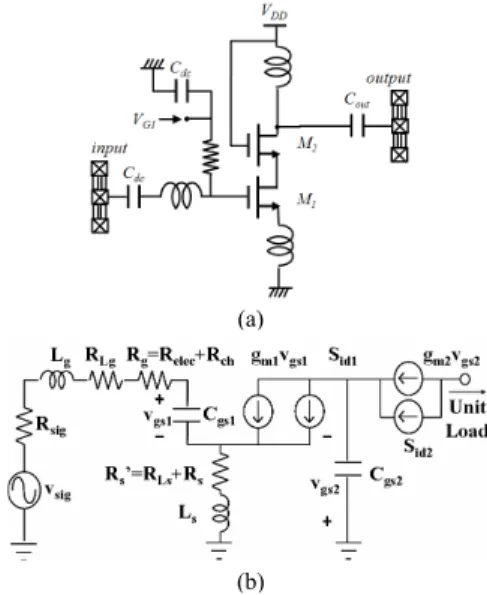
683 LNAs schematic and its small signal equivalent circuit with Cgd consideration are shown in Fig. 1. As scaling down the technology, the effect of the C
gdcan not be ignored any more especially at mm-wave frequency range. From that equivalent circuit, the input matching condition (Re[Z
in], Im[Z
in]) and noise figure equation (NF-1) can be derived as equations (1)-(3) [7]. The channel thermal noise, Sid, is analytically modeled as equation (4).
In equation (1), R
1is the sum of the parasitic
resistance of the gate inductor, gate electrode resistance of transistor, and the sum of parasitic resistance of the source inductor and transistor source resistance. Q-factor of inductors is assumed as 10 to extract the parasitic resistance. For the convenience, we call the 1st, the 2nd and the 3rd term of noise figure equation (3) as resistor, M1 transistor and M2 transistor noise term, respectively.
The dominant term of noise figure varies for frequency range as explained in the next section. In other word, there are two cross point among three terms. These points varies with device width and process nodes.
Therefore, design approach should be changed based on the target operating frequency and the process node to be used.
(a)
(b)
(c)
Fig. 2 At 60nm gate length, device width vs. (a) resistor
term, (b) M1 transistor term, and (c) M2 transistor term (a)(b)
Fig. 1 (a) Schematic of inductively degenerated common-
source cascode LNA. (b) Small signal equivalent circuit of (a)한국정보통신학회논문지 Vol. 24, No. 5: 682-685, May. 2020
684
Ⅲ. Noise Analysis
Fig 2-(a), (b), (c) show each term in NF equation (3) for width variations as frequency increases. The resister noise term decrease as width increases to meet matching condition. On the contrary, both the transistor noise terms increase as width increases. The increasing of the width of transistors requires 1/ω
2C
gsto be decreased and R
1also decreases. Therefore, the resistor term decreases as the width increases. Otherwise, transistor terms increase as width increases because S
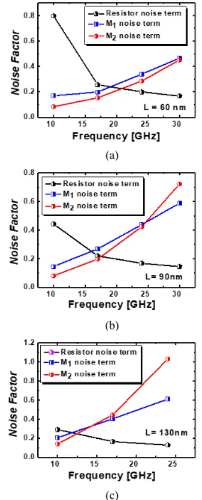
idis proportional to IDS [8]. Consequently, the dominant noise term varies as frequency changes and its tendency for different process are shown in Fig 3-(a), (b), (c).
(a)
(b)
(c)
Fig. 3 Each noise term vs. frequency for gate length of
(a) 60nm, (b) 90nm, and (c) 130nm.There are two cross points among three noise terms.
We call the cross points as 1st and 2nd transition frequency where dominant noise term is changed from resistor term to M1 transistor term and from M1 transistor term to M2 transistor term, respectively. As the gate length decreases, both transition points increase for the same device width. Since gate resistance which mainly attributes to resistor noise term increases as gate length decreases, the 1st transition point increases as gate length decreases. On the other hand, cut-off frequency f
Tincreases as gate length decreases.
Therefore, the 2nd transition point increases as gate length decreases. Considering the width variation, both transition points vary as shown in Fig. 4-(a),(b).
(a)
(b)
Fig. 4 (a) The first transition frequency, and (b) the
second transition frequency vs. width.The gate resistance decreases as device width increases while the transistor noise terms increase.
Therefore, the 1st transition point becomes lower as the
width increases. However, the 2nd transition point is
almost flat for the width variation. Because cut-off
frequency of each device is almost same even with the
width variation if the gate length is the same. In addition,
Cgd 성분을 포함한 공정별 주요 잡음원 천이과정 연구
685 S
idof both transistor terms increase proportional to width. Based on the results, we can claim the following design strategy. The Q-factor and gate resistance which largely contribute on the resistor noise term are most important factors at lower frequency than the 1st transition point. Furthermore, the conventional cascode topology has no more advantages in terms of noise at higher frequency than the 2nd transition point. At low frequency for example, the larger width of device can reduce the noise more by reducing the gate resistance.
However, if the larger width of device is used, the lower 1st transition frequency is obtained. Consequently, using large width of device for reducing noise is only effective below the 1st transition frequency.
Ⅳ. Conclusion
In this paper, we analyze noise figure of LNAs for frequency and width variations. Also we explored the noise transition point for gate length variation. Two transition points vary for frequency and width and show the different tendency with the different gate length.
Based on the results, we could claim that the conventional cascade topology has only advantages in noise performance until the operating frequency is lower than the 2nd transition point. Also, we verified that using larger width of device to reduce the noise is only effective below the 1st transition frequency.
REFERENCES
[ 1 ] A. M. Niknejad, S. Thyagarajan, E. Alon, Y. Wang, and C.
Hull, "A circuit designer's guide to 5G mm-wave." in
Proceeding of IEEE Custom Integrated Circuits Conference (CICC), pp. 1-8, Sep. 2015.
[ 2 ] X. S. Loo, Moe Z. Win, K. S. Yeo, “fT Enhancement of CMOS Transistor Using Isolated Polysilicon Gates.” in
Proceeding of IEEE Radio Frequency Integrated Circuits Symposium (RFIC), pp. 76-79. 2018.
[ 3 ] Y. Cheng, "A study on figures of merit for high frequency behavior of MOSFETs in RF IC applications." in Proceeding
of Workshop Compact Modeling, 2005.
[ 4 ] I. Song, J. Jeon, H. S. Jhon, J. Kim, B. G. Park, J. D. Lee, and H. Shin, "A simple figure of merit of RF MOSFET for low-noise amplifier design." IEEE Electron Device Letters, vol. 29, pp 1380-1382, 2008.
[ 5 ] P. Qin, and X. Quan, "Design of wideband LNA employing cascaded complimentary common gate and common source stages." IEEE microwave and wireless components letters, vol. 27, pp. 587-589, 2017.
[ 6 ] M. Arsalan, and W. Falin "LNA Design for Future S Band Satellite Navigation and 4G LTE Applications." Computer
Modeling in Engineering & Sciences, vol. 119, pp 249-261,
2019[ 7 ] H. Jung, H. S. Jhon, I. Song, M. Koo, and H. Shin, "Design optimization of a 10 GHz Low Noise Amplifier with gate drain capacitance consideration in 65 nm CMOS Technology."
in Proceeding of IEEE 9th International Conference on
Solid-State and Integrated-Circuit Technology, pp. 1480-
1483, Oct. 2008.[ 8 ] J. Jeon, J. D. Lee, B.-G. Park, and H. Shin, “An analytical channel thermal noise model for deep sub-micron MOSFETs with short-channel effects,” Solid-State Electronics, vol. 51, no. 7, pp. 1034-1038, July 2007.