논문 2009-46SD-10-10
고속 LVDS 응용을 위한 전송선 분석 및 설계 최적화
( Analysis and Design Optimization of Interconnects for High-Speed LVDS Applications )
류 지 열*, 노 석 호**
* ( Jee-Youl Ryu and Seok-Ho Noh )
요 약
본 논문에서는 고속 저전압 차동 신호(Low-Voltage Differential Signaling, LVDS) 전송방식의 응용을 위한 전송선 분석 및 설계 최적화 방법을 제안한다. 차동 전송 경로 및 저전압 스윙 방법의 발전으로 인해 저전압 차동 신호 전송방식은 데이터 통 신 분야, 고 해상도 디스플레이 분야, 평판 디스플레이 분야에서 매우 적은 소비전력, 개선된 잡음 특성 및 고속 데이터 전송 률을 제공한다. 본 논문은 차동 유연성 인쇄 회로 보드(flexible printed circuit board, FPCB) 전송선에서 선 폭, 선 두께 및 선 간격과 같은 전송선 설계 변수들의 최적화 기법을 이용하여 직렬 접속된 전송선에서 발생하는 임피던스 부정합과 신호 왜곡을 감소시키기 위해 개선 모델과 개발된 수식을 제안한다. 이러한 차동 FPCB 전송선의 고주파 특성을 평가하기 위해 주파수 영 역에서 전파(full-wave) 전자기 시뮬레이션 및 시간 영역 시뮬레이션을 각각 수행하였다. 본 논문에서 제안하는 방법은 저전압 차동 신호 방식의 응용을 위한 고속 차동 FPCB 전송선을 최적화하는데 매우 도움이 되리라 믿는다.
Abstract
This paper addresses the analysis and the design optimization of differential interconnects for high-speed Low-Voltage Differential Signaling (LVDS) applications. Thanks to the differential transmission and the low voltage swing, LVDS offers high data rates and improved noise immunity with significantly reduced power consumption in data communications, high-resolution display, and flat panel display. We present an improved model and new equations to reduce impedance mismatch and signal degradation in cascaded interconnects using optimization of interconnect design parameters such as trace width, trace height and trace space in differential printed circuit board (FPCB) transmission lines. We have carried out frequency-domain full-wave electromagnetic simulations, and time-domain transient simulations to evaluate the high-frequency characteristics of the differential FPCB interconnects. We believe that the proposed approach is very helpful to optimize high-speed differential FPCB interconnects for LVDS applications
Keywords : Low-Voltage Differential Signaling (LVDS), differential transmission, flexible PCB (FPCB), high-speed
I. Introduction
Recently consumers are demanding higher display
*
정회원, 부경대학교 전자컴퓨터통신공학부
(Division of Electronic, Computer and
Telecommunication Engineering Pukyong National University)
**
정회원, 안동대학교 전자공학과
(Major of Electronic Engineering, College of Electronic & Information Engineering, Andong National University)
접수일자: 2009년7월27일, 수정완료일: 2009년9월29일
resolutions and higher color depths of the LCDs in mobile and flat panel display applications. With this increase in demand for higher performance, current technologies are becoming less efficient due to the limited data rates and power dissipation. With Low-Voltage Differential Signaling (LVDS), which is a new technology addressing the needs of today's high performance data transmission applications, data rate has increased tremendously to meet these demands in the high bandwidth market and still consumes much less power than competing
technologies[1~5]. The LVDS standard is now becoming the most popular high-speed differential data transmission standard in the industry, because it offers low power, low-noise coupling, low electromagnetic interference (EMI) emissions, switching capability beyond many current standards, and ability to be integrated into system level ICs[6~10]. This LVDS technology also allows products to address high data rates ranging from 100 Mbps to greater than 2 Gbps. Transmission data speeds arrived to some hundreds of MHz and are approaching to 1GHz. Transferring of data at such high speed between boards or systems, demands a meticulous design of the traces and ground plane, as transmission line with controlled characteristic impedance.
Flexible printed circuit boards (FPCBs) have become the preferred media for mobile applications as flexible, multifunctional, compact and light components[1, 5~6]. The flexibility is achieved by producing thin conductors above thin layers of dielectric materials. Fig. 1 shows a typical structure of a FPCB. Because of its dimension, there is no reliable model for designing transmission lines with controlled impedance for FPCB.
The reliable analysis and optimized design of the high-speed differential FPCB transmission lines are still important to reduce impedance mismatch and signal degradation[4~6]. Controlled characteristic impedance of a stack-up in high-speed systems is the most critical parameter in FPCB design. This
Cover layer
Cover layer Adhesive
Adhesive Conductors
Conductors Dielectric material 1mil
1.4mil
2mil
1.4mil
1mil
그림 1. FPCB의 대표적인 구조 Fig. 1. A typical structure of a FPCB.
impedance determines signal quality such as reflections, crosstalk, and mismatch between transmitters and receivers[5].
In this work, we describe the analysis and the design optimization of differential FPCB transmission lines for high-speed LVDS applications. An improved model and new equations to reduce impedance mismatch and signal degradation in cascaded interconnects are presented. This model optimizes design parameters such as trace width, trace height and trace space in differential FPCB transmission lines. To analyze the high-frequency characteristics of the differential FPCBs, we evaluated characteristic impedance, differential impedance, reflection coefficient, and near-end crosstalk coefficient using frequency‐domain full‐wave electromagnetic simulations.
Ⅱ. Interconnects Analysis and Optimization
2.1. LVDS Overview and Link
LVDS uses differential signals of the opposite polarity with low voltage swings to transmit data at high rates[8~9]. Fig. 2 illustrates simplified diagram of LVDS. LVDS outputs consist of a current source with normal 3.5mA that drives the differential pair lines. The basic receiver has a high DC input impedance, so the majority of driver current flows across the 100 Ω termination resistor generating
그림 2. LVDS 전송방식에 대한 단순화된 개념도 Fig. 2. Simplified diagram of LVDS.
about 350 mV across the receiver inputs. The termination resistor provides a path between the complementary signal paths of the system. When the transmitter switches, it changes the direction of current flow across the resistor, thereby creating a valid “one” or “zero” logic state.
2.2. Transmission Line Analysis
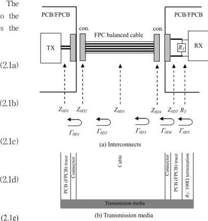
Let's consider FPCB interconnects for transmission media with 50 Ω connectors as shown in Fig. 3.
Interconnects consist of FPCB traces in TX and RX parts and FPC cable. At the receiver, a 100 Ω termination resistor is used to match the impedance of the transmission line that connects the receiver to the driver. Closely matching the impedance of this termination resistor with the impedance of the transmission lines reduces significantly harmful signal reflections that decrease signal quality. When characteristic impedance of each interconnect is not equal (said to be mismatched), there is reflection of the incident wave. Equations (2.1a) to (2.1e) show reflection coefficients for each interconnect. The amplitude of the reflected wave normalized to the amplitude of the incident wave is known as the reflection coefficient, Γ:
G
0 1 0 2 0 10 2 0 1
D
D D
D D
Z Z
Z Z
= -
+ (2.1a)
G
0 0 3 0 20 3 0 2
D
D D
D D
Z Z
Z Z
2
= -
+ (2.1b)
G
0 3 0 4 0 30 4 0 3
D
D D
D D
Z Z
Z Z
= -
+ (2.1c)
G
0 4 0 5 0 40 5 0 4
D
D D
D D
Z Z
Z Z
= -
+ (2.1d)
G
0 5 0 50 5 D
T D
T D
R Z
R Z
= -
+ (2.1e)
where
Z
0D1 toZ
0D5 represent interconnectimpedances.
When the lines are perfectly matched, Γ=0 with no reflected wave. It is recommended that all impedances should be within 10% of the target impedance in 100 Ω to minimize any reflections. The TX and RX should be located as close to the interface as possible as shown in Fig. 3. This is done to minimize the FPCB LVDS overall trace length and thus skew as well. Skew is generally proportional to length, thus a shorter interconnect nominally has less skew associated with it. To obtain good signal integrity and signal quality for overall interfaces between TX and RX, we need to avoid unnecessary via, sharp bends or other discontinuities.
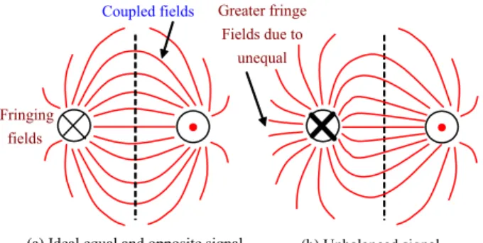
For LVDS, the DC currents should never flow in the same direction, but factors can cause an imbalance in currents shown in Fig. 4(b) as compared to the ideal case in Fig. 4(a).
When this imbalance happens, an excess of field fringing occurs since the field strength of the two conductors is unequal. The extra fringe field can
PCB/FPCB
TX
con.
PCB/FPCB
RX FPC balanced cable
con.
R
TZ
0D1Z
0D2Z
0D3Z
0D4Z
0D5R
TG
0D1G
0D2G
0D3G
0D4G
0D5(a) Interconnects
(b) Transmission media
PCB (FPCB) trace Connector Cable
Transmission media
Connector PCB (FPCB) trace RT: 100W termination
그림 3. 전송 매체 간 상호 결합 특성 Fig. 3. Interconnects for transmission media.
Coupled fields
(a) Ideal equal and opposite signal Fringing
fields
(b) Unbalanced signal Greater fringe
Fields due to unequal
그림 4. 차동 전송선에 대한 오드 모드 신호 Fig. 4. Odd mode signals on differential lines.
escape as TEM waves and lead to more EMI. At GHz frequencies, any discontinuity due to this impedance mismatch will cause severe degradation in signal integrity, especially in low‐voltage signaling systems such as LVDS. To achieve good impedance matching, the transmission line analysis of the intended interconnect structure with the accurate modeling in FPCB should be carried out.
2.3. Development of Improved Model and New Equations
This paper presents an improved model and newly developed equations for FPCB.
Let’s make a FPCB model considering a typical FPCB structure shown in Fig. 1. Fig. 5 shows an improved model for FPCB with buried coupled micro-strip structure. This model contains polyimide (PI) and adhesive (epoxy) with dielectric constant
e
r2 on the conventional coupled micro-strip structure. It also has a thin polyimide film as a dielectric base material.Fig. 6 shows differential-mode excitations for a coupled line and its equivalent capacitance networks.
e
r1h
1w s w
t
+
-e
r2Cu
PI + Adhesive (Epoxy)Dielectric material (PI)
h
2그림 5. FPCB에 대한 매몰 결합형 마이크로 스트립 모 델
Fig. 5. Buried coupled micro-strip model for FPCB.
E-wall
+I -I
C
11C
222C
122C
12그림 6. 결합 전송선에 대한 차동 모드 방사 및 등가 커패시턴스 회로
Fig. 6. Differential-mode excitations for a coupled line and equivalent capacitance networks.
Newly developed equations using an improved FPCB model can be extracted from this equivalent capacitance circuit. If we assume a TEM type of propagation, then the electrical characteristics of the coupled lines can be completely determined from the effective capacitances between the lines and velocity of propagation on the line. Balanced differential lines have equal but opposite (“odd” mode) signals. This means that the concentric magnetic field lines tend to be canceled and the electric fields tend to be coupled.
The capacitances of two conductors are a function of the field lines orbit. As shown in Fig. 6, one orbit group consists of vertical field lines between signal trace and ground plane. The other orbit group provides horizontal or lateral field lines between the two traces. For the odd mode, the electric field lines have an odd symmetry for the center line, and a voltage null exists between the two strip conductors.
We can imagine this as a ground plane through the middle of
C
12, which leads to the equivalent circuit as shown in Fig. 6.C
12 represents the capacitance the two strip conductors in the absence of the ground conductor, whileC
11 andC
22 represent the capacitances between the oneeach strip conductor and ground in the absence of the other strip conductor. In this case, the resulting capacitance of either line to ground for the odd mode isC
o= C
11+ 2 C
12= C
22+ 2 C
12(2.2)
and the differential impedance isZ
diff= vC 1
o(2.3)
where
v
is signal transmission velocity of line. The value ofZ
diff can be determined by calculating the capacitanceC
0.Now let us describe newly developed equations using improved FPCB model and its equivalent circuit shown in Figs. 5 and 6, and equations (2.2) to (2.3).
Equations (2.4a) and (2.4b) express the characteristic impedance and the differential impedance for a burred micro-strip structure, respectively. Equation (2.4a) is known in [11], and equation (2.4b) is newly developed for FPCB.
Z h
r
w t
0 1
87 1
1 41 5 98
= 0 8
+ +
æ
èç ö
ø÷
e
. ln ..
(2.4a)
Z Z ws h w t
ws h w t
r r
r r r
diff = + +
+ +
2 5
0 15
1 1 2
1 1 1 2
e e
e e e
( )
. ( )
(2.4b)
where
e
r1 ande
r2 are dielectric constants for base film PI and buried layer (PI + adhesive), respectively. Parametersh
1,w
,t
ands
represent PI thickness, trace width, trace thickness and distance between the traces of a pair, respectively.Coupled noise, or crosstalk, is the electric noise caused by mutual inductance and capacitance between signal traces due to their close proximity to each other. If not controlled through proper design, crosstalk can cause high-speed digital system failure due to false signals appearing on the transmission lines. Equation (2.5a) is known in [1, 8], and equation (2.5b) is modified from equation known in [11].
Far-end or forward crosstalk is usually not a problem in buried micro-strip environments, so in our approach we We considered near-end or backward crosstalk. If the coupled trace is perfectly well terminated at the near-end with the characteristic impedance of the trace (
Z
0), there will be a little reflection at the near -and a little backward crosstalk reflecting back down the line.CT w s h
T t
Tol Z Tol R
NE
RT r
=
T+ + × æ
è ç ö
ø ÷ × + 1
1
122
0
[( ) / ]
( ) ( )
(2.5a)
T
RT= × × 2 l 85 0 475 .
er1+ 0 67 . (2.5b)
whereCT
NE is near-end or backward crosstalk coefficient,T
RT is the round trip propagation time, andt
r is signal rising time.Tol
(Z
0) andTol
(R
T) are tolerances forZ
0 andR
T, respectively, andl
is trace length. TheT
RT/t
r term cannot exceed 1.0, and the final term applies only if there are terminations at both ends of the traces.These equations are available for narrow micro-strips. Use these equations from (2.4a) to (2.5b) when 0.1<
w
/h
<2.0 and also when 1<e
r1 ande
r2<15.Ⅲ. Results And Discussion
“Timing” is very important factor in a high-speed system. Signal timing depends on the shape of the waveform when the threshold is reached. Signal waveform distortions can be caused by two mostly concerned noise problems such as reflection noise and crosstalk noise. The reflection noise is due to impedance mismatch, stubs, vias and other interconnect discontinuities. The electromagnetic coupling between signal traces and vias results in crosstalk noise. In this section, results for these important parameters using an improved FPCB model and developed equations are described for differential FPCB transmission line.
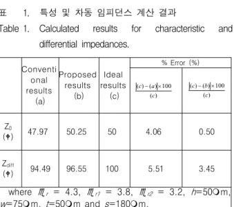
3.1 Characteristic and Differential Impedances
Table 1 lists calculated results for characteristic and differential impedances to verify accuracy of proposed equations (2.4a) and (2.4b). Equations for conventional results are referred to [12]. As shown in Table 1, proposed equations showed accurate results as compared to conventional results.Fig. 7(a) shows the effect of trace thickness for
Conventi onal results (a)
Proposed results
(b)
Ideal results (c)
% Error (%)
) (
100 ) ( ) (
c a c- ´
) (
100 ) ( ) (
c b c- ´
Z
0(W) 47.97 50.25 50 4.06 0.50
Z
diff(W) 94.49 96.55 100 5.51 3.45
where
er= 4.3,
er1= 3.8,
er2= 3.2,
h=50mm,
w=75mm,
t=50mm and
s=180mm.
표 1. 특성 및 차동 임피던스 계산 결과
Table 1. Calculated results for characteristic and differential impedances.
20% variation (of nominal value) in the trace width of FPCB differential interconnects on characteristic and differential impedances. The effect of trace thickness for -50% to +150% changes in the trace space of differential interconnects on characteristic and differential impedances is shown is in Fig. 7(b).
The reference or nominal value has been designed to obtain characteristic and differential impedances of approximately 50 ohm and 100 ohm, respectively. The key parameters are depicted in Figs. 7(a) and (b).
The simulations have been performed at 500 MHz.
The results are obtained using equations (2.4a) and (2.4b).
As shown in Fig. 7(a), the 10% change in trace width produced change of approximately 6% in differential impedance for trace thickness of 17.5 μm.
The differential impedance for trace thickness of 35 μ m showed change of about 5.6% from its reference value. As expected from equations (2.4a) and (2.4b), the differential impedance showed noticeable changes for increased trace thickness. The 50% change in the trace space showed change of less than 1% in the differential impedance. However, the characteristic impedance did not changed as shown in equations (2.4a) and (2.4b). When the trace space increases from its reference value, the differential impedance also increases. As shown in Figs. 7(a) and (b), it can be observed that the effect of trace thickness is more significant than any other parameters. The differential
(a)
(b)
그림 7. (a) 전송선 폭 비 및 (b) 전송선 간 거리 비에 따른 특성 임피던스 및 차동 임피던스 변화 Fig. 7. The effect of (a) trace width ratio and (b) trace
space ratio of differential interconnects on characteristic and differential impedances.
impedance showed the slight change in the trace space as compared to the variation in the trace width.
3.2. Reflection Coefficient
Figs. 8(a) and (b) show the effect of trace thickness for changes in the trace width and space of FPCB differential interconnects on reflection coefficient. The reflection is mostly caused by impedance mismatch. The effect of the signal reflection is one of most concerned noise problems in a high-speed serial interface system. The results shown in Fig. 8 are obtained using Fig. 7 and
(a)
(b)
그림 8. (a) 전송선 폭 비 및 (b) 전송선간 거리 비에 따 른 반사계수 및 차동 반사계수의 변화
Fig. 8. The effect of (a) trace width ratio and (b) trace space ratio of differential interconnects on reflection coefficients.
equation (2.1e). From these results, we can analyze general problem for reflection of a normally incident wave at the interface of a mismatch impedance of the material.
As shown in Figs. 8(a) and (b), the trace structure with trace thickness of 35 μm showed large reflection as compared to trace thickness of 17.5 μm.
This means that the trace structure with thinner conductor is much better than that with thicker conductor in FPCB differential interconnect environments. It can be expected that when the trace widths increase, the reflection coefficients increase, and the trace spaces increase, the reflection
coefficients decrease.
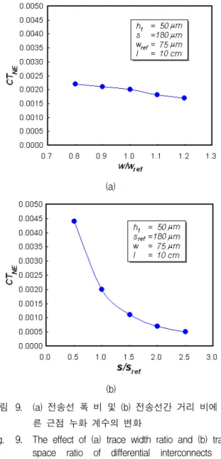
3.3. Near-End Crosstalk Coefficient
The effect of trace thickness for changes in the trace width and space of FPCB differential interconnects on crosstalk is shown in Fig. 9. It is assumed that the tolerances for
Z
0 andR
T are 10%, and signal rising time is 2ns. The results shown in Fig. 9 are obtained using equations (2.5a) and (2.5b).Crosstalk margin can be defined by
Crosstalk Coefficientç£ 0.005. (3.1)
As shown in Figs. 4 and 6, the two signal traces(a)
(b)
그림 9. (a) 전송선 폭 비 및 (b) 전송선간 거리 비에 따 른 근점 누화 계수의 변화
Fig. 9. The effect of (a) trace width ratio and (b) trace space ratio of differential interconnects on near-end crosstalk coefficients.
are coupled by the electric field, resulting in crosstalk. The degree of crosstalk between two adjacent signal conductors depends on their proximity to each other. Consequently, the maximum crosstalk allowed for a given differential interconnect determines the maximum space between conductors, and thus, determining the minimum allowable signal line space. As can be seen from Figs. 9(a) and (b), typical signal conductor space in FPCB can be more than 180 mm to reduce crosstalk to an acceptable level. It is expected that as the trace space increases, the mutual inductance and capacitance decrease, and thus the crosstalk noise level decreases.
Ⅳ. Conclusions
We have analyzed and optimized high-speed differential FPCB transmission lines for LVDS. An improved FPCB model and new equations were developed. We have performed frequency-domain full-wave EM simulations, and time-domain transient simulations, and S-parameter simulations. Design guidelines were established from results such as trace width, trace height and trace space in differential FPCB. The results for important parameters such as differential impedance, reflection coefficient and crosstalk coefficient were discussed.
We expect that the proposed approach is very useful to optimize and design high-speed serial interface FPCB interconnects for LVDS applications.
References
[1] J.‐Y. Ryu and S.‐H. Noh, “Analysis and Design Optimization of Interconnects for High-Speed LVDS Applications,”
Conference of the Korean Institute of Maritime Information &
Communication Science
, Vol. 11, No. 2, pp.761-764, October 2007.
[2] D. Chowdhury et. al., “Analysis of differential termination technique in cascading of high-speed LVDS signals on a PCB,”
Procs. of the IEEE INDICON‐First India Annual Conference
, pp.557-560, Dec. 2004.
[3] X. Fan et. al., “ The performance improvement of via structure in LVDS by optimizing partial widths of the traces,”
Procs. of ICMMT 4th International Conference on Microwave and Millimeter Wave Technology
, pp. 398‐401, Aug.2004.
[4] S. Ahn et. al., “Solution space analysis of interconnects for low voltage differential signaling (LVDS) applications,”
Electrical Performance of Electronic Packaging
, pp. 327‐330, Oct. 2001.
[5] M. M. Mechaik, “An evaluation of single‐ended and differential impedance in PCBs,”
International Symposium on Quality Electronic Design
, pp. 301‐306, Mar. 2001.[6] E. Recht and S. Shiran, “A simple model for characteristic impedance of wide microstrip lines for flexible PCB,”
IEEE International Symposium on Electromagnetic Compatibility
, pp. 1010‐1014, Aug. 2002.[7] IEEE standard for Low‐Voltage Differential Signals (LVDS) for Scalable Coherent Interface (SCI),
IEEE Std 1596.3‐1996
, July 1996.[8] National Semiconductor,
Application Note 1085
, June 1999.[9] J.‐Y. Lee et. al., “A 400Mbps/ch SiDP receiver for mobile TFT‐LCD driver IC,”
SID 06
, pp.1499‐1501, June 2006.
[10] J. Goldie, “LVDS goes the distance,”
SID 99
, pp.1‐4, June 1999.
[11] H. W. Johnson and M. Graham, High-Speed Digital Design: A Handbook of Black Magic, Prentice Hall PTR, New Jersey, p. 186‐221.
[12] http://focus.ti.com/lit/ug/sllu039/sllu039.pdf.
저 자 소 개
류 지 열
(정회원)He received BS and MS degrees in 1993 and 1997 from Pukyoug National University in Dept. of Electronic Engineering, Busan, South Korea, respectively. He received Ph.D degree in 2004 from Arizona State University in Dept. of Electrical Engineering, Tempe, United States of America. He was worked with Samsung SDI Co., Ltd in 2005. Since 2009, he is a full-time instructor at Pukyoug National University in Division of Electronics, Computer and Telecommunication Engineering. His current research interests include ubiquitous communication system-on-chip design, RF IC design and testing, MMIC design and testing, and analog IC desing and testing. He also has interests for passive modeling, testing and analysis, and RF MEMS technology.
노 석 호
(정회원)He received B. Eng. Degree in electronic engineering from Hanyang University, Seoul, Korea, in 1982 and M. Eng.
Degree in information
engineering from Tokyo Institute of Technology, Tokyo, Japan in 1990, and the Ph.D degree in information engineering from the Saitama National University, Saitama, Japan, in 1993. In 1993 he joined Satellite Communication Division of ETRI as a research staff. Since 1998, he is an Professor at Andong National University, Andong, Korea. In 2003 he was a Visiting Researcher at the Dept. of Electrical Engineering of the Arizona State .