Vol. 30, No. 9 (2020)
441
Zinc Oxide Nanostructured Thin Film as an Efficient Photoanode for Photoelectrochemical Water Oxidation
Jong-Hyun Park and Hyojin Kim †
Department of Materials Science and Engineering, Chungnam National University, Daeduk Science Town, Daejeon 34134, Republic of Korea
(Received July 13, 2020 : Revised August 12, 2020 : Accepted August 20, 2020)
Abstract
Synthesizing nanostructured thin films of oxide semiconductors is a promising approach to fabricate highly efficient photoelectrodes for hydrogen production via photoelectrochemical (PEC) water splitting. In this work, we investigate the feasibility as an efficient photoanode for PEC water oxidation of zinc oxide (ZnO) nanostructured thin films synthesized via a simple method combined with sputtering Zn metallic films on a fluorine-doped tin oxide (FTO) coated glass substrate and subsequent thermal oxidation of the sputtered Zn metallic films in dry air. Characterization of the structural, optical, and PEC properties of the ZnO nanostructured thin film synthesized at varying Zn sputtering powers reveals that we can obtain an optimum ZnO nanostructured thin film as PEC photoanode at a sputtering power of 40 W. The photocurrent density and optimal photocurrent conversion efficiency for the optimum ZnO nanostructured thin film photoanode are found to be 0.1 mA/cm2 and 0.51 %, respectively, at a potential of 0.72 V vs. RHE. Our results illustrate that the ZnO nanostructured thin film has promising potential as an efficient photoanode for PEC water splitting.Key words
oxide semiconductor, zinc oxide, nanostructure, photoanode, photoelectrchemical water splitting.1. Introduction
We regard harvesting sunlight to provide clean chemical fuels such as hydrogen as a desirable and sustainable approach toward meeting future demands for energy with minimal environmental impact.
1-3)Several different approaches have been attempted to the development of advanced processes for the production of hydrogen from the solar-driven splitting of water. Among these approaches,
4-6)it is well known that photoelectrochemical (PEC) water splitting is one of the most promising hydrogen generation techniques in a highly efficient and eco-friendly way. Generally, solar-driven water splitting process includes two half-cell reactions of the water oxidation or hydrogen evolution reaction (HER) and the water reduction or oxygen evolution reaction (OER), and thus the process requires the separation of water oxidation and reduction reactions.
7)Therefore, because PEC cells spatially separate HER and OER, those cells are widely used as solar-driven water splitting devices.
The main reason why the selection and design of the
photocatalytic materials for the water oxidation and reduction photoelectrodes are crucial in a PEC cell system is that the capability of the PEC cell for water splitting is largely determined by the light absorption and subsequent carrier transport in the photoelectrodes.
8)So far, it has been revealed that oxide semiconductors such as zinc oxide (ZnO), titanium dioxide (TiO
2), hematite (Fe
2O
3), cuprous oxide (Cu
2O) and cupric oxide (CuO) show a promising potential as photoelectrodes for solar- driven hydrogen production.
9-12)Among them, ZnO has been another promising material of much attention as a photoanode for water oxidation since Fujishima and Honda discovered the phenomenon of PEC water splitting on a TiO
2photoanode in 1972.
13)As an n-type oxide semiconductor with a wide direct band gap of 3.3 eV at 300 K,
14)ZnO has the valence band edge lower than the water oxidation potential and is thus supposed to work as a photoanode for water oxidation through taking electrons from water molecules under light illumination.
However, the large band gap energy of ZnO limits its solar-driven water splitting for hydrogen production due
†
Corresponding author
E-Mail : [email protected] (H. Kim, Chungnam Nat’l Univ.)
© Materials Research Society of Korea, All rights reserved.
This is an Open-Access article distributed under the terms of the Creative Commons Attribution Non-Commercial License (http://creative-
commons.org/licenses/by-nc/3.0) which permits unrestricted non-commercial use, distribution, and reproduction in any medium, provided the
original work is properly cited.
material ZnO. In this respect, ZnO nanostructures including nanowires and nanorods are considered to be much promising for an enhancement in the PEC performance owing to their great surface-to-volume ratio.
16)Here we attempt to synthesize ZnO nanostructured thin films by a simple method combined with sputtering Zn metallic films and subsequent thermal oxidation of the sputtered Zn films in dry air, because a large scale of uniform metallic Zn films is expected to be deposited easily by sputtering.
17)In the present work, we report on the feasibility as an efficient photoanode for PEC water oxidation of ZnO nanostructured thin films synthesized via a simple method combined with sputtering Zn metallic films on a fluorine- doped tin oxide (FTO) coated glass substrate and subsequent thermal oxidation of the sputtered Zn metallic films in dry air. The fabricated ZnO nanostructured thin film photoanode is shown to exhibit the PEC water oxidation performance as good as the vertically aligned ZnO nanorod array photoanode, illustrating that the rather simple ZnO nanostructured thin film is a promising photocatalytic material for an efficient photoanode in a PEC cell system.
2. Experimental Procedure
ZnO nanostructured thin films were prepared with the use of a Zn nanoparticle layer formed via two consecutive steps.
17)First, Zn metal films were grown on a glass substrate coated with a fluorine tin oxide (FTO) electrode from a pure Zn target by a rf sputtering method in an Ar atmosphere of 5 mTorr during 8 min at varying sputtering power of 10~40 W, beyond which no Zn nanoparticle layer was formed due to high sputtering power. The substrate temperature was kept at 100 ºC and the substrate-to-target distance was set to be 12 cm.
Second, the as-sputtered Zn films were then thermally oxidized in dry air at a temperature of 400 ºC for 1 hour using a rapid thermal annealing system with the initial increasing rate of the annealing temperature being kept at 20 ºC/min.
The crystalline structures of the ZnO nanostructured thin films were characterized by X-ray diffraction (XRD) using Cu K
αradiation along with Raman spectroscopy, and then their microstructures were analyzed by scanning electron microscopy (SEM). The optical properties of the ZnO nanostructured thin films were examined by UV-
photoanode were performed in a three-electrode cell with our photoanode as the working electrode, a Pt sheet as counter electrode, and a Ag/AgCl reference electrode with an aqueous 1 mM Na
2SO
4solution pH-adjusted to 6.6 as the electrolyte. The area of the photoanode exposed to light was 0.5 × 1.0 cm
2. The photoresponse was measured under a continuous irradiation from a 300 W Xe lamp, and the light intensity were calibrated to 1 mW/cm
2for the incidence onto the photoanode.
3. Results and Discussion
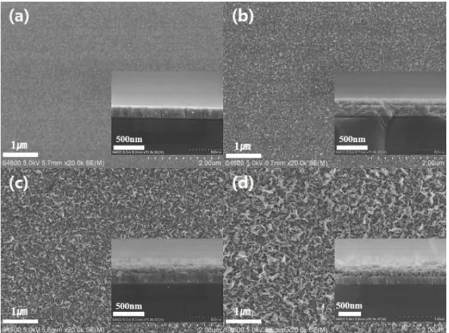
We present typical SEM images of the ZnO nano- structured thin films prepared on FTO-coated glass substrate for different Zn sputtering powers of 10, 20, 30, and 40 W in Fig. 1. Here it should be note that we could not obtain any ZnO nanostructured thin film for Zn sputtering power above 50 W since no Zn nanoparticle layer was formed due to high sputtering power. It is clearly seen from Fig. 1 that flower-like ZnO nanostructured thin films are properly formed except for the case of the Zn sputtering power of 10 W. The estimated thicknesses of the prepared ZnO thin films for the Zn sputtering power of 20, 30, and 40 W are, respectively, 94, 120, and 205 nm. As the Zn sputtering power increases in the range between 20 and 40 W, the ZnO nanostructured thin film is found to have a rougher surface and more complex texture. The observed change in morphology of the prepared ZnO thin films for the Zn sputtering power of 20, 30, and 40 W can be attributed to formation of the nanoparticle layer with different size distribution of the Zn nucleation sites corresponding to the Zn sputtering power.
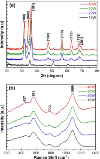
X-ray diffraction (XRD) was used to verify the
formation of the ZnO crystalline phase. Fig. 2(a) shows
typical XRD patterns of the ZnO nanostructured thin
films prepared on FTO-coated glass substrate for different
Zn sputtering powers of 10, 20, 30, and 40 W. It is
clearly seen from Fig. 2(a) that the observed diffraction
peaks for the cases other than Zn sputtering power of 10
W simply correspond to the hexagonal wurtzite ZnO
crystalline phase (JCPDS card no. 36-1451) and no
diffraction peaks of second phases were detected, indicating
the successful preparation of the polycrystalline ZnO
nanostructured thin films of the single phase. It is noted
here that the XRD peaks for the case of the Zn sputtering
power of 10 W partly come from the substrate due to an
incomplete covering the substrate by the prepared film, as clearly seen from the corresponding SEM image in Fig. 1.
The formation of the ZnO crystalline phase can be further confirmed by the Raman spectroscopy analysis.
Fig. 2(b) shows the Raman spectra of the ZnO nano- structured thin films prepared on FTO-coated glass substrate for different Zn sputtering powers of 10, 20, 30, and 40 W. In these observed spectra at room temperature, three distinct lines at 437, 574, 1,090 cm
−1correspond to the characteristic phonon frequencies of ZnO crystalline phase while one distinct line at 773 cm
−1comes from the substrate. For the observed Raman lines from ZnO phase, the line at 437 cm
−1is assigned to the E
1(TO) phonon mode, the line at 574 cm
−1is ascribed to the A
1(LO) phonon mode, and the line at 1,090 cm
−1is due to the acoustic combination of A
1and E
2phonon modes.
18)Also, it is found from these observed results that the characteristics of the Raman spectrum of the prepared ZnO nanostructured thin film are not sensitive to the Zn sputtering power. Consequently, both the observed XRD and Raman spectroscopy results demonstrate the successful preparation of the ZnO nanostructured thin films.
Fig. 3 shows the UV-vis-NIR absorbance spectra of the
ZnO nanostructured thin films prepared on FTO-coated glass substrate for different Zn sputtering powers of 10, 20, 30, and 40 W. It is clearly seen from Fig. 3 that the ZnO nanostructured thin films have an absorption edge at about 450 nm due to the high band gap energy of ZnO. As observed in the Raman spectrum measurement, it is found that the characteristics of the UV-vis-NIR absorbance spectrum of the prepared ZnO nanostructured thin films are also insensitive to the Zn sputtering power.
Usually, Tauc plot, which is obtained from UV-vis-NIR spectra, is used to determine the band gap energy of semiconductor based on the following equation:
19)( αhν)
n= A(hν − E
g)
where α is the absorption coefficient which can be obtained
from UV-vis-NIR spectra, hν is the energy of photon, A
is a constant, E
gis the optical band gap energy, and
exponent n is dependent on the nature of the optical
transition. It is known that n is 2 for direct transition and
n is 1/2 for indirect transition.
20)As shown in the inset of
Fig. 3, straight line is obtained when ( αhν)
2is plotted
against photon energy ( hν), indicating that the absorption
is due to a direct transition for ZnO. The estimate band
Fig. 1. Typical top-view and cross-sectional SEM images of the flower-like ZnO nanostructured thin films prepared on FTO-coated glass
substrate for the Zn sputtering power of (a) 10 W, (b) 20 W, (c) 30 W, and (d) 40 W.
gap energy of the ZnO nanostructured thin film prepared for the Zn sputtering power of 40 W, which can be obtained from the intercept on the abscissa, is 3.32 eV. This estimated value is in good agreement with the previous standard value for ZnO.
14)It is noted that the estimated band gap energy of the prepared ZnO nanostructured thin film slightly decreases as increasing the Zn sputtering power.
The PEC water oxidation performance of the fabricated ZnO nanostructured thin flim photoanode was characterized through the current density−potential ( J−V) response curve measured using the linear sweep voltammetry under white light illumination. Fig. 4(a) shows the J−V response curves of the ZnO nanostructured thin film photoanodes fabricated for different Zn sputtering powers of 10, 20, 30, and 40 W. It is clearly seen from Fig. 4(a) that the J−V response curve of the ZnO nanostructured thin film photoanode fabricated for the Zn sputtering power of 40 W exhibits the steepest increase in current with respect to the potential and thus has the best performance of the PEC water oxidation. The observed enhancement in the PEC water oxidation performance
could be ascribed to an increase in surface roughness of the ZnO nanostructured thin film, as revealed in Fig. 1, Fig. 2. (a) Typical X-ray diffraction patterns and (b) Raman spectra
of the ZnO nanostructured thin films prepared on FTO-coated glass substrate for various Zn sputtering powers.
Fig. 3. Optical absorption spectra of the ZnO nanostructured thin films prepared on FTO-coated glass substrate for various Zn sputtering powers. The inset shows the Tauc plot for the prepared ZnO nanostructured thin films.
Fig. 4. (a) Measured current density and (b) estimated photo-
conversion efficiency (PCE) curves of the ZnO nanostructured thin
film photoanodes under an applied voltage for various Zn
sputtering powers.
which is supposed to result in an increase in the effective surface reaction area.
The photocurrent conversion efficiency (PCE) for photoelelctrochemical water oxidation of the photoanode were estimated from our observed J−V characteristic data using the following equation:
21)PCE (%) =
Here, E
RHE[V] is the applied external potential vs. a reversible hydrogen electrode (RHE), J
p[mA/cm
2] is the externally measured current density at E
RHEunder light illumination, P
i[mW/cm
2] is the power density of the incident light, and 1.23 [V] is the potential for water splitting reaction. The applied potentials were measured vs. Ag/AgCl reference electrode and converted to the RHE scale using the Nernst function:
22)E
RHE= E
Ag/AgCl+ E
0Ag/AgCl+ 0.059 pH
Here, E
RHEis the converted potential vs. RHE, E
Ag/AgClis the external potential measured against the Ag/AgCl reference electrode, E
0Ag/AgClis the standard electrode potential of the Ag/AgCl reference electrode (0.1976 V vs. RHE at 25
oC),
8)and pH is the acidity of the solution.
Fig. 4(b) presents the estimated PEC curves of the ZnO nanostructured thin film photoanodes under an applied voltage vs. RHE for various Zn sputtering powers. As expected from the observed PEC response characteristics in Fig. 4(a), the ZnO nanostructured thin film photoanode for the Zn sputtering power of 40 W is found to exhibit a significantly higher photocurrent conversion efficiency.
Consequently, it is confirmed that the ZnO nanostructured thin film photoanode exhibits the optimal photocurrent conversion efficiency of 0.51 % and the corresponding photocurrent density of 0.1 mA/cm
2at a potential of 0.72 V vs. RHE (that is, 0.14 V vs. Ag/AgCl), which are as nearly high as those of the ZnO nanorod array photoanode (0.49 % and 0.13 mA/cm
2at 0.85 V vs. RHE).
23)These photoelectrochemical results convincingly demonstrate that the ZnO nanostructured thin film photoanode can possess the photocurrent conversion efficiency as good as an one-dimensional ZnO nanostructure photoanode at a somewhat lower applied potential.
The long-term stability of the ZnO nanostructured thin film photoanode was tested by obtaining the photocurrent density−time ( J−t) response curve. Fig. 5 shows the photo- current responses of the flower-like ZnO nanostructured thin film photoanodes fabricated for different Zn sputtering powers of 20, 30, and 40 W at a bias voltage of 0 V vs.
Ag/AgCl with white light chopped (on/off) during each 20 sec. It is seen from Fig. 5 that no photocurrent is in
the dark. When the white light was illuminated, the photocurrent climbed promptly and then gradually reached a stable state. The observed behavior is associated with the photogenerated electrons under white light radiation, the recombination of photogenerated electron–hole pairs, and the balance of generation and recombination of electron–hole pairs.
11)The observed photocurrent densities after 40 sec for different Zn sputtering powers of 20, 30, and 40 W were decreased to 78, 83, and 83 % values of their respective initial photocurrent densities, suggesting their long-term stability to be addressed.
4. Conclusions
In summary, the flower-like ZnO nanostructured thin film photoanodes fabricated through thermal oxidation of sputtered Zn films in dry air at low temperature exhibited an efficient PEC water oxidation performance. From the characterization of the structural, optical, and PEC properties of the ZnO nanstructured thin film prepared for different Zn sputtering powers, it was revealed that we could obtain the optimum ZnO nanostructured thin film as PEC photoanode at a sputtering power of 40 W. The photocurrent density and optimal photocurrent conversion efficiency for the optimum ZnO nanostructured thin film photoanode were found to be 0.1 mA/cm
2and 0.51 %, respectively, at a potential of 0.72 V vs. RHE, which are as good as those of the vertically oriented ZnO nanorod array photoanode. Our results illustrate that the ZnO nanostructured thin film has promising potential as an efficient photoanode for PEC water splitting.
Acknowledgements
This work was supported by the Basic Science Research through the National Research Foundation of
Jp×(1.23 E– RHE)Pi
--- ×100
Fig. 5. (a) Photocurrent responses of the ZnO nanostructured thin
film photoanodes at a bias voltage of 0 V vs. Ag/AgCl with white
light chopped (on/off) for each 20 sec.
S. A., 103, 15729 (2006).
2. P. V. Kamat, J. Phys. Chem. C, 111, 2834 (2007).
3. C.-J. Winter, Int. J. Hydrogen Energy, 34, S1 (2009).
4. A. Kudo and Y. Miseki, Chem. Soc. Rev., 38, 253 (2009).
5. F. E. Osterloch, Chem. Soc. Rev., 42, 2294 (2013).
6. X. Chen, S. Chen, L. Guo and S. S. Mao, Chem. Rev., 110, 6503 (2010).
7. Y. Yang, D. Xu, Q. Wu and P. Diao, Sci. Rep., 6, 30158 (2016).
8. Y. Liu, Y. Gu., X. Yan, Z. Kang, S. Lu, Y. Sun and Y.
Zhang, Nano Res., 8, 2891 (2015).
9. M. Y. Wang, L. Sun, Z. Q. Lin, J. H. Cai, K. P. Xie and C. J. Lin, Energy Environ. Sci., 6, 1211 (2013).
10. D. A. Wheeler, G. M. Wang, Y. C. Ling, Y. Li and J. Z.
Zhang, Energy Environ. Sci., 5, 6682 (2012).
11. Z. Kang, Y. S. Gu, X. Q. Yan, Z. M. Bai, Y. C. Liu, S.
Liu, X. H. Zhang, Z. Zhang, X. J. Zhang and Y. Zhang, Biosens. Bioelectron., 64, 499 (2015).
12. Z. Kang, X. Q. Yan, Y. F. Wang, Z. M. Bai, Y. C. Liu, Z. Zhang, P. Lin, X. H. Zhang, H. G. Yuan and X. J.
Zhang, Sci. Rep., 5, 7882 (2015).
13. A. Fujishima and K. Honda, Nature, 238, 37 (1972).
14. V. Srikant and D. R. Clarke, J. Appl. Phys., 83, 5447
18. R. Zhang, P. G. Yin, N. Wang and L. Guo, Solid State Sci., 11, 865 (2009).
19. J. Tauc, R. Grigorovici and A. Vancu, Phys. Status Solidi B, 15, 627 (1966).
20. P. Sinsermsuksakul, J. Heo, W. Noh, A. S. Hock and R.
G. Gordon, Adv. Energy Mater., 1. 1116 (2001).
21. T. Hisatomi, J. Kubota and K. Domen, Chem. Soc. Rev., 43, 7520 (2014).
22. D. T. Sawyer, A. J. Sobkowiak and J. Roberts, Jr., Electrochemistry for Chemists, p.196, 2nd ed., John Wiley & Sons, New York (1995).
23. J.-H. Park and H. Kim, Korean J. Mater. Res., 30, 239 (2020).
Author Information Jong-Hyun Park
충남대학교 신소재공학과 박사과정 학생
Hyojin Kim
충남대학교 신소재공학과 교수