DOI: http://dx.doi.org/10.4313/JKEM.2016.29.1.30 ISSN 1226-7945 (Print), 2288-3258 (Online)
N-polar면의 선택적 에칭 방법을 통한 Free-standing GaN 기판의 Bowing 제어
김진원
1,3
, 손호기
1
, 임태영
1
, 이미재
1
, 김진호
1
, 이영진
1
, 전대우
1,a
, 황종희
1
, 이혜용
2
, 윤대호
3
1 한국세라믹기술원 광·디스플레이소재 센터
2 루미지엔테크
3 성균관대학교 신소재공학부
Control of Bowing in Free-standing GaN Substrate by Using Selective Etching of N-polar Face
Jinwon Gim
1,3, Hoki Son
1, Tea-Young Lim
1, Mijai Lee
1, Jin-Ho Kim
1, Young Jin Lee
1, Dae-Woo Jeon
1,a, Jonghee Hwang
1, Hae-Yong Lee
2, and Dae-Ho Yoon
3
1
Optic & Display Materials Team, Korea Institute of Ceramic Engineering & Technology, Jinju
52851, Korea
2 LumiGNtech, Gwangmyeong 14322, Korea
3 School of Advanced Materials Science & Engineering, Sungkyunkwan University, Suwon 16419, Korea
(Received November 23, 2015; Revised December 16, 2015; Accepted December 21, 2015)
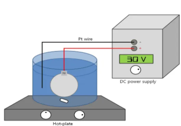
Abstract: In this paper, we report that selective etching on N-polar face by EC (electro-chemical)-etching effect on the
reduction of bowing and strain of FS (free-standing)-GaN substrates. We applied the EC-etching to concave and convex
type of FS-GaN substrates. After the EC-etching for FS-GaN, nano porous structure was formed on N-polar face of
concave and convex type of FS-GaN. Consequently, the bowing in the convex type of FS-GaN substrate was decreased but
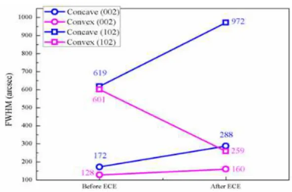
the bowing in the concave type of FS-GaN substrate was increased. Furthermore, the FWHM (full width at half maximum)
of (1 0 2) reflection for the convex type of FS-GaN was significantly decreased from 601 to 259 arcsec. In the case, we
confirmed that the EC-etching method was very effective to reduce the bowing in the convex type of FS-GaN and the
compressive stress in N-polar face of convex type of FS-GaN was fully released by Raman measurement.
Keywords: GaN, Electro-chemical etching, Bowing, Freestanding GaN, Wet process
1. 서 론
GaN은 청색과 자외선 영역의 레이저 다이오드(laser diode)나 발광 다이오드(light emitting diode)와 같은
Copyright ©2016 KIEEME. All rights reserved.
This is an Open-Access article distributed under the terms of the Creative Commons Attribution Non-Commercial License (http://creativecommons.org/licenses/by-nc/3.0) which permits unrestricted non-commercial use, distribution, and reproduction in any medium, provided the original work is properly cited.
광전자기기에 적합한 재료로 각광받고 있다. 게다가 넓
은 직접 밴드갭(wide direct band gap)과 높은 열전
도도 가지며 고온에서 작동하는 전자기기에 적용되어
질 수 있다 [1]. FS-GaN (free-standing GaN) 기판은
고품질 GaN 성장을 위한 homo-epitaxial 성장을 할
수 있기 때문에 bulk GaN을 대체할 수 있다고 알려져
있다 [2]. 수소화물기상증착법 (hydride vapor phase
epitaxy, HVPE)은 고품질의 FS-GaN 단결정을 제공하고
다른 bulk 성장법(high-pressure solution growth,