제 2 회 첨단 사이언스 교육 허브 개발(EDISON) 나노물리 경진대회
Characterization of SWCNT Field Effect Transistor via Edison Simulation
Mingxing Piao, Sang-Jin Lee, In-Yeob Na
School of Electrical Engineering, Korea University, Anam-Dong, Sungbuk-Ku, Seoul 136-713, Korea e-mail: [email protected], [email protected], [email protected]
ABSTRACT: A semiconducting single-walled carbon nanotube (SWCNT) field-effect transistor (FET) in a top-gate model was constructed. The effect of different high- κ dielectric materials (Al 2 O 3 , HfO 2 and HfSiON) and various temperatures with a wide range from 50K to 500K on the performance of such nominal device were investigated. Several key device parameters including the on/off ratio of the current, transconductance (g m ), subthreshold swing, and carrier mobility were used to evaluate the device performance. The simulated results fit well with the experiment results previously published.
INTRODUCTION
In recent years, there has been much interest in the investigation of the performance of field-effect transistors (FETs) based on individual semiconducting single-walled carbon nanotube (SWCNT), which is a prime candidate for many applications in nano electronics[1-2]. The performance of SWCNT based FETs is not only influenced by the electronic properties of channel materials, but also related with the geometric structure of device and environment conditions.
However, due to the complicated technology process, especially for the n-type doped SWCNTs, it is difficult to obtain the optimized device condition. Hence, it is helpful to take a theretical calculation before the device fabrication, which also could make a performance comparison with the prepared devices. Here, by employing Edison Nano Physics simulation tool, the current-voltage (I-V) curves were simulated under the different conditions and the corresponding key parameters were discussed to evaluate the device performance.
METHODS
The nominal device has a semiconducting SWCNT (13,0) as the channel material with n-type characteristics. The diameter of the SWCNT taking consider as the channel width was calculated according to the equation below:
d= a 0 • (m 2 + mn + n 2 ) 1/2 /π (1) where a 0 where was the atomic lattice constant (0.246nm) [3];
The gate voltage was swept from -1.0V to 1.0V with a fixed supply voltage of 500 mV. The channel length was selected as 10 nm. Two conditons were simulated including high- κ dielectric material and temperature. In the case of high-κ dielectric material, the nominal device was a top-gate FET model except SiO 2 , which a back- gate model was constructed as the reference device.
In the case of temperature, a wide temperature range from 50K to 500K was considered. The schematic of the nominal device was shown in Fig.
1.
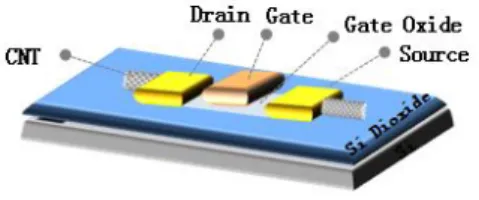
Fig. 1. Schematic of the nominal device with a top-gate structure.
The performance of the nominal device was estimated using several key device parameters including the on/off current ratio, transconductance (g m ), subthreshold swing (S) and carrier mobility (μ). The transconductance is defined as
g m = δ I ds / δ V gs (2) The subthreshold swing is defined as
S= δ V gs / δ(log I ds ) (3) Where V gs is the gate voltage and I ds is the source- drain current;
62 260
제 2 회 첨단 사이언스 교육 허브 개발(EDISON) 나노물리 경진대회
The carrier mobility is given by
μ = g m • L/ C• V sd (4) where g m is the transconductance, L is the channel length, C is the gate capacitance, and V sd is the source-drain voltage applied.
Since the individual SWCNT was used as the channel material, the gate capacitance was empolyed by C g1 [4], which is defined as
C g1 = 2 π• κ• ε 0 / ln (4t/d) (5) Where κ is dielectric constant, the ε 0 is vacuum dielectric constant, t is the dielectric thickness and d is the CNT diameter.
RESULTS AND DISCUSSION
As previously reported [5], top-gate models of CNT FETs using high-κ dielectric material as the gate insulator have several advantages for integrated circuit application. Top-gated CNT FETs allow local gate biasing at low voltage, high integration density and high speed switching. It is useful to explore how the high- κ dielectric material affects the device performance of the nominal SWCNT FET. The bottom-gate FET model with SiO 2 as the gate insulator (thickness:
300nm) was used as the reference device. Three kinds of high-κ material including Al 2 O 3 , HfO 2 , HfSiON were selected for top-gate FET model fabrication with the thicknesses setting at 30nm, 2.5nm and 2.5nm, respectively.
Fig. 2 shows the typical gate transfer characteristics at room temperature with a fixed V sd =500 mV. In the case of SiO 2 as the dielectric material, on-current I on =1.45×10 -5 A, and off- current I off =8.23×10 -10 A, giving this device an on/off ratio =1.8×10 4 . The subthreshold slope was 205 mV/dec and transconductance 16 μS∣ Vds=500
mV . When the SiO 2 gate insulator was replaced by Al 2 O 3 , HfO 2 or HfSiON, the values of on-current I on were 3.19×10 -5 A, 5.76×10 -5 A, 6.23×10 -5 A, respectively, the corresponding off-current I off
values are 1.08×10 -10 A, 7.02×10 -10 A,7.02×10 -10 A, which resulted the on/off ratio 3.0×10 7 , 8.2×10 6 , 8.9×10 6 , respectively. Furthermore, the calculated subthreshold swings were 119, 79.9 and 65.4 mV/dec. The tansconductance are 47, 105 and 108
μS∣ Vds=500 mV . According to the present results
above, it shows clearly that the usage of high- κ
dielectric material with a top-gate configuration has a much better performance with respect to reference devices. The carrier mobility of each device was also calculated, as seen in Fig. 3.
Compared with the reference values of 104.2 cm 2 ·V -1 ·s -1 , the carrier mobility of top-gated FET was 89.5, 58.2 and 47.8 cm 2 ·V -1 ·s -1 , respectively.
Taking consider that using a high- κ dielectric material as the gate insulator demands a much smaller dielectric thickness than that of SiO 2 , resulting a relative larger values of capacitance, which takes a dominant effect on the carrier mobility. Though it possessed a higher transconductance, the carrier mobility was decreased instead.
Fig. 2. Current voltage characteristics of n-doped SWCNTs FET with different gate dielectric materials, the inset shows in log scale.
Fig. 3. a) Different gate dielectric materials dependent on-and off-state current; b) On/off ratio vs different gate dielectric materials; c) Transconductance vs different gate dielectric materials; d) Subthreshold swing vs different gate dielectric materials.
63 261
제 2 회 첨단 사이언스 교육 허브 개발(EDISON) 나노물리 경진대회
Fig. 4. Mobility vs different gate dielectric materials.
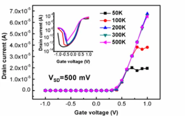
Next, the effect of temperature on the device performance was investigated. A wide temperature region from 50K to 500K was selected. The typical gate transfer characteristics at different temperature with a fixed V sd =500 mV was shown in Fig. 5. At T=300K (room temperature), the on state current is 6.60×10 -5 A and off state current is 1.43×10 -12 A yielding a on/off ratio of 4.6×10 7 . When the temperature was up to 500K, the FET still shows typical n-type field-effect characteristics but with degraded performance. In particular the on/off current ratio dropped to 7.3×10 6 , which resulted mainly from the slight decrease of the on-state current and the drastic increase of the off-state current. The decrease of the on-state current is mainly from the increased phonon scattering at higher temperature. Whereas, the increased off current is governed by thermal activation of the carriers across the potential barrier which is exponentially dependent on temperature [6-7]. On the other hand, in the low temperature range (from 50K to 200K), the on- state current was increased from 3.19×10 -5 A to 6.75×10 -5 A and the highest current level raised at 200K. However, the off-state current at 50K was almost one order of magnitude smaller than that of at 200K, the highest on/off ratio was appeared at the lowest simulated temperature (50K). The transconductance (g m ) showed the same trend as the on-state current, which was increased in the low temperature range (50K to 200K) and then decreased (200K to 500K). Subthreshold swing is an important temperature-dependent parameter for characterizing the switching property of FET devices [8]. The extracted subthreshold swing
values of the nominal devices at various temperatures were presented in Fig. 6(d). With the temperature increasing, the values of subthreshold swing were also increased, which was accorded with the experiment results previously published.
In principle, the subthreshold swing may be improved via increasing the gate capacitance by optimizing the gate material and structure. In fact, this was proved by the simulation results above.
Last, the carrier mobility of each device was also calculated. From the equation (4), we could see clearly that except of g m , other parameters including L, C, and V sd are all fixed; hence the carrier mobility is determined by the values of g m
in the case of temperature. The carrier mobility was changed with the same trend as transconductance. The highest carrier mobility was about 54 cm 2 ·V -1 ·s -1 at 200K.
Fig.5. Current voltage characteristics of n-doped SWCNTs FET with different temperatures, the inset shows in log scale.
Fig. 6. a) Temperature dependent on-and off-state current; b) On/off ratio vs temperature; c) Transconductance vs temperature; d) Subthreshold swing vs temperature.
64 262
제 2 회 첨단 사이언스 교육 허브 개발(EDISON) 나노물리 경진대회