정시켜둔 p(a-Si)층의 도핑농도 값을 조정하면 더 높은 효율을 기대할 수 있을 것이다.
ACKNOWLEDGEMENT
이 논문은 2015도 정부(교육과학기술부)의 재원 으로 한국연구재단- 첨단 사이언스
교육 허브 개발 사업(EDISON)의 지원을 받아 수 행된 연구입니다.
REFERENCES
[1] M. Tanaka, et al, “Development of Mew a-Si/c- Si Heterojunction Solar Cells : ACJ-HIT (Artificially Constructed Junction-Heterojunction with Intrinsic
Thin-Layer)”, Appl. Phys., 31 3518-3522 (1992) [2] Y. Matsumoto et al., “A new type of high efficiency with a low-cost solar cell having the structure of a μc-SiC/polycrystalline silicon heterojunction” J. Appl. Phys., 67, 6538 (1990).
[3] https://nano.edison.re.kr
[4] Y.Tsunomura, et al, “Twenty-two percent efficiency HIT solar cell”, Solar Energy Materials and Solar Cells, 93 670-673 (2009)
[5] Q.Wang, et al, “crystal silicon heterojunction solar cells by hot-wire CVD”, IEEE Photovoltaic Specialists Conference, 33 1-5 (2008)
Analysis of Quantum Effects Concerning Ultra-thin Gate-all-around Nanowire FET for Sub 14nm Technology
이한결, 김성연, 박재혁
Department of Electrical Engineering, KAIST, 305-701 Daejeon, Republic of Korea E-mail:
[email protected], [email protected], [email protected]
In this work, we investigate the quantum effects exhibited from ultra-thin GAA(gate-all- around) Nanowire FETs for Sub 14nm Technology. We face designing challenges particularly short channel effects (SCE). However traditional MOSFET SCE models become invalid due to unexpected quantum effects. In this paper, we investigated various performance factors of the GAA Nanowire FET structure, which is promising future device. We observe a variety of quantum effects that are not seen when large scale. Such are source drain tunneling due to short channel lengths, drastic threshold voltage increase caused by quantum confinement for small channel area, leakage current through thin gate oxide by tunneling, induced source barrier lowering by fringing field from drain enhanced by high k dielectric, and lastly the I-V characteristic dependence on channel materials and transport orientations owing to quantum confinement and valley splitting. Understanding these quantum phenomena will guide to reducing SCEs for future sub 14nm devices.
INTRODUCTION
The 10nm technology for semiconductor device fabrication would follow 14nm technology node, which is mentioned on International Technology Roadmap for Semiconductors (ITRS). The 14nm technology is reached on 2014 and now we are facing on 10nm technology.
As the device geometry goes smaller, sub-14nm technology will face more severe short channel effects (SCEs), as same as past technology development. To manage the challenges, we analysed multigate structure, channel length, channel area, oxide thickness, oxide material, channel material, channel orientation, which might affect on SCEs, in this work.
CALCULATION METHODS
To obtain I-V characteristics, software tool named
“Software for Nanowire FET device performance and characteristic analysis” on EDISON nanophysics website was used.
The simulation tool adopted non-equilibrium Green’s function (NEGF) approach. With nearly-free electron approximation, solution is based on the parabolic effective mass theory[1]. Therefore, input material data can be expressed by effective masses and used to solve self-consistent equations quantum-mechanically.
The parameter definitions to investigate performances are shown in the following table 1.
RESULTS AND DISCUSSION 1. Effect of Multigate Structure
The Tri-gate structure is adopted for the current
Vt (Threshold voltage) Vg @ Id = 100nA
DIBL(Drain Induced Barrier Lowering)
SS(Subthreshold Slope) SS = @Vg<Vt
Table 24. Parameter definitions used in this work
Fig. 1. Multigate FET structures
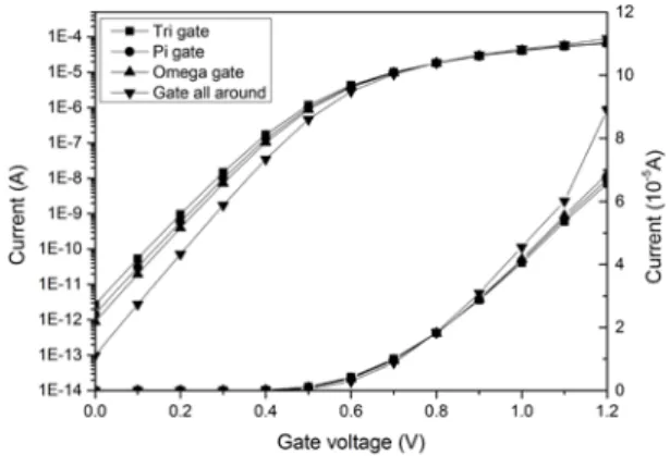
22nm and 14nm technology. Its multigate structure reduces short channel effects more than the previous FET structures such as ultrathin-body silicon-on-oxide (UTB SOI) MOSFET, double-gate (DG) FET and Fin FET. Some multigate structures, PI, Omega, and gate-all-around (GAA) structures have been reported, which is described in Fig. 1.
From the result shown in Fig. 2. The minimum SCE is observed on GAA structure, for gate length (Lg) = 10nm. Omega, PI and Tri-gate FET is following. This is consistent result to [2].
Since the performance of GAA was predominant among the other multigate structures, it is expected
to be a psomising device structure in the future.
Fig. 2. I-V characteristics of multigate structures
Therefore, the following simulations ware carried out using GAA FETs as a default structure.
2. GAA Nanowire FET as Default Structure The following simulation experiments were based on a gate-all-around silicon nanowire FET (GAA Si NW FET) structure. Detailed variables are shown in Table. 2.
The channel length (=gate length) is 10nm since we focus on the next generation 10nm technology.
The channel area is 5nm 5nm, namely ultra-thin ( 5nm) which cause quantum mechanical effect. The default channel doping type is intrinsic (undoped).
The oxide material is silicon oxide with thickness of 1nm, from effective oxide thickness (EOT) value from ITRS 2014. The default transport orientation is (100)/[001]. The resons for the default values will be discussed in following subsections.
2.1 Effect of Channel Length
Even though the GAA FET has strong immunity to SCEs, it still shows SCE depending on channel length. The SCE of GAA FETs were calculated varying the channel lengths. The result is represented in Fig 3. Short channel effect GAA FETs 67
The Tri-gate structure is adopted for the current
Vt (Threshold voltage) Vg @ Id = 100nA
DIBL(Drain Induced Barrier Lowering)
SS(Subthreshold Slope) SS = @Vg<Vt
Table 24. Parameter definitions used in this work
Fig. 1. Multigate FET structures
22nm and 14nm technology. Its multigate structure reduces short channel effects more than the previous FET structures such as ultrathin-body silicon-on-oxide (UTB SOI) MOSFET, double-gate (DG) FET and Fin FET. Some multigate structures, PI, Omega, and gate-all-around (GAA) structures have been reported, which is described in Fig. 1.
From the result shown in Fig. 2. The minimum SCE is observed on GAA structure, for gate length (Lg) = 10nm. Omega, PI and Tri-gate FET is following. This is consistent result to [2].
Since the performance of GAA was predominant among the other multigate structures, it is expected
to be a psomising device structure in the future.
Fig. 2. I-V characteristics of multigate structures
Therefore, the following simulations ware carried out using GAA FETs as a default structure.
2. GAA Nanowire FET as Default Structure The following simulation experiments were based on a gate-all-around silicon nanowire FET (GAA Si NW FET) structure. Detailed variables are shown in Table. 2.
The channel length (=gate length) is 10nm since we focus on the next generation 10nm technology.
The channel area is 5nm 5nm, namely ultra-thin ( 5nm) which cause quantum mechanical effect. The default channel doping type is intrinsic (undoped).
The oxide material is silicon oxide with thickness of 1nm, from effective oxide thickness (EOT) value from ITRS 2014. The default transport orientation is (100)/[001]. The resons for the default values will be discussed in following subsections.
2.1 Effect of Channel Length
Even though the GAA FET has strong immunity to SCEs, it still shows SCE depending on channel length. The SCE of GAA FETs were calculated varying the channel lengths. The result is represented in Fig 3. Short channel effect GAA FETs
start to appear around 10nm and become
Structure GAA
Channel (=Gate) Length 10nm
Channel Area 5nm 5nm
Channel Material Si
Channel Doping Intrinsic (Un-doped) Channel Transport 100
Oxide Thickness 1nm Oxide Material SiO2 (
Table 2. Default input parameters used for simulations
Figure 3. I-V characteristics varying by channel length
noticeable at 5nm, which is expressed in Table 3.
In the case of the 5nm gate length case from above figure, relatively large amount of current flows when gate voltage equals to zero. The potential profile and transported energy level is expressed in Fig. 4.
It is remarkable that transport energy level is below channel conduction band level. It implies the dominant principle of the drain current is tunneling mechanism.
From result above, it is reasonable to assume that for the gate lengths lower than 10nm, source-drain
tunnelling of electron increases and leads to large
Channel
length 5nm 10nm 15nm 20nm
Threshold voltage (mV)
57.2 440 502 520
Table 25. Threshold voltages calculated extracted from channel length variation simulation
Figure 26. Tunneling phenomena observed at 10nm channel length
amount of off current and degradation of subthreshold slope. This source-drain tunnelling might be obstacle when scaling below 10nm.
Therefore, the following simulations was performed aiming to reduce the SCE of the 10nm GAA FET.
2.2 Effect of Channel Area
The channel area 5nm 5nm is considered as
“ultra-narrow” for silicon nanowire (SiNW) which is smaller than 5nm sqare cross-section. Electrical and Optoelectronic properties of SiNWs can be changed by dopant concentration, and quantum effects such as quantum confinement and valley splitting for width less than or equal to 5nm.
From the result of Fig. 5, short channel effects of GAA FETs emerges around 10nm and become nontrivial at 5nm. This is due to ‘quantum mechanical narrow channel effect’. Electrons occupy discrete energy levels in the channel. From lateral confinement, the lowest energy level is certain
value higher above the bottom of the conduction
Figure 27. I-V characteristcs depending on channel area
Figure 28. Conduction band energy level profile and current density due to the quantum
confinement
((a),(c) Lch=2nm, (b), (d) Lch=1nm)
band by energy level quantization. This requires larger surface potential for inversion layer population, such that threshold voltage increases
The quantum confinement gets severe when channel length shrinks from 2nm into 1nm. The potential profile information is in Fig. 6. In the case of 1nm channel length, conduction band level of channel become higher than 2nm case, even though the same gate and drain voltage were
applied.
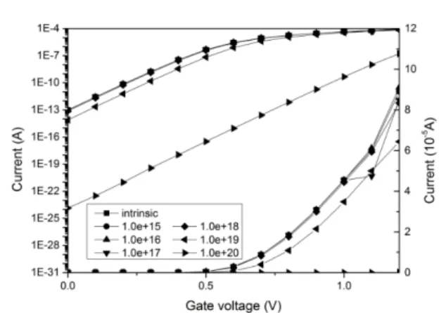
Figure 29. I-V characteristcs depending on channel doping concentration.
2.3 Impact of Channel Doping
Traditionally, for planar MOSFETs, the purpose of channel doping was to adjust the threshold voltage, using the equation below.
The intrinsic (undoped) channel is selected according to [3]. This paper describes that there is more variation in drain current when high channel doping is inflicted. With the MOSFET gate length (=channel length) shorter than 100nm, random dopant fluctuation arises by imperfect control of doping, resulting threshold voltage variation more than conventional theory as channel doping increases. The intrinsic (undoped) channel can evade this random dopant induced fluctuation while also achieving reduced impurity scattering and increased mobility. Although channel doping implies these practical issues, the simulation assumes the doping concentration is homogeneous in the channel area. Based on this knowledge, we calculated the effects on channel doping illustrated on Fig 7.
2.4 Effect of Oxide Thickness 69
value higher above the bottom of the conduction
Figure 27. I-V characteristcs depending on channel area
Figure 28. Conduction band energy level profile and current density due to the quantum
confinement
((a),(c) Lch=2nm, (b), (d) Lch=1nm)
band by energy level quantization. This requires larger surface potential for inversion layer population, such that threshold voltage increases
The quantum confinement gets severe when channel length shrinks from 2nm into 1nm. The potential profile information is in Fig. 6. In the case of 1nm channel length, conduction band level of channel become higher than 2nm case, even though the same gate and drain voltage were
applied.
Figure 29. I-V characteristcs depending on channel doping concentration.
2.3 Impact of Channel Doping
Traditionally, for planar MOSFETs, the purpose of channel doping was to adjust the threshold voltage, using the equation below.
The intrinsic (undoped) channel is selected according to [3]. This paper describes that there is more variation in drain current when high channel doping is inflicted. With the MOSFET gate length (=channel length) shorter than 100nm, random dopant fluctuation arises by imperfect control of doping, resulting threshold voltage variation more than conventional theory as channel doping increases. The intrinsic (undoped) channel can evade this random dopant induced fluctuation while also achieving reduced impurity scattering and increased mobility. Although channel doping implies these practical issues, the simulation assumes the doping concentration is homogeneous in the channel area. Based on this knowledge, we calculated the effects on channel doping illustrated on Fig 7.
2.4 Effect of Oxide Thickness
Oxide thickness
5nm 10nm 15nm 20nm
SS (mV/dec)
62.08 64.57 67.56 70.71
Table 4. Subthreshold slope calculated by varying oxide thickness
Figure 30. I-V characteristcs depending on oxide thickness
The two largest reasons for shortening gate oxide thickness is to reduce short channel effects, and to drive high current at a small gate voltage.
From the results of Fig 8 and Table 4, we predict that the subthreshold swing reduces as oxide thickness reduce. This is due to equation SS = , where (per area) decrease as tox increase. Also threshold increase
since .
However, below 1nm, direct tunnelling dramatically increase the gate leakeage current as oxide thickness reduces. This results increase of static power consumption. In order to overcome this issues, high-k dielectrics are used as substitutes to SiO2, which increases equivalent oxide thickness
Figure 9. I-V characteris depending on oxide materials
Figure 31. Source potential barrier lowered by fringing field
(EOT) for the same physical thickness.
2.5 Effect of High K Oxide Material From the issues mentioned above in the case of oxide thickness, high-k materials are selected as alternatives for SiO2. One of the widely used high- k dielectric is hafnium oxide (HfO2), since HfO2 mitigate the Vth shift hysteresis phenomenon attributed to charge trappings, which are commonly observed by high-k integration. Simulations were
carried SiO2 gate oxide by such high-k dielectrics, here represented by HfO2 ( .
The results of Fig. 9 differs from the expectations from the tradition planar MOSFET model where
SS = .
According to the equation, oxide with high-k dielectric will result larger Cox and smaller SS.
However, the outcome turn out to be opposite, high-k HfO2 having higher SS value than SiO2.
This is due to stronger capactive coupling between drain and channel due to the high-k gate dielectric. The fringe capacitance due to fringing field increase by the squre of
. This field is observed from the simulated result shown in Fig 10.
Drain electrode is more tightly coupled to the channel, resulting strong short channel effect.
Electrons encounter lower barrier entering the channel from the source side for HfO2. Although off current Ioff increase due to SS degradation, HfO2 exhibits higher on current. Although high-k HfO2 has smaller electron mobility due to surface phonon scattering and Coulomb scattering, the stronger capactive coupling between drain and channel enhances the carrier density at the source.
2.6. Effect of Multigate Structure
The channel material is one of the most important factors influencing device performance.
Currently, Si is the most dominant channel material in the industry. Since its properties have been proved experimentally to show high performance, it has been adopted as a channel material from past bulk devices. However, as device geometry gets smaller, other materials like Ge are emerging and suggest possibilities for high-performance ultra- thin 2D or 1D devices [4]. According to this, we have
Figure 32 I-V characteristics varying crystal orientations
Crystal
orientaion (100) (110) (111)
Drain current (@ Vg=1.0V)
(μA) 45.5 38.5 34
Table 5. Drain current at 1.0V gate voltage depending on crystal orientation
to consider which material shows better performance in an extremely scaled NW device. We simulated three types of channel materials for ultra- thin GAA NW with a 5nm* 5nm cross-section, 10- nm-gate-length geometry.
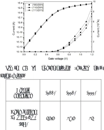
To investigate the dependence on crystal orientation, simulations were performed for orientations of (100)/[001], (110)/[001], (111)/[110], which denote the mostly used current channel materials in 5nm-square-cross-section Si NWs.
From its results in Fig 11, Table 5, the (100)/[001]
channel orientation shows the best performance for the simulated geometry. For further scaling, there are possibilities that a (110) orientation might be better when Si is the channel material [5].
For the channel material simulation, we selected Si, Ge, GaAs as samples. However, the simulation 71
carried SiO2 gate oxide by such high-k dielectrics, here represented by HfO2 ( .
The results of Fig. 9 differs from the expectations from the tradition planar MOSFET model where
SS = .
According to the equation, oxide with high-k dielectric will result larger Cox and smaller SS.
However, the outcome turn out to be opposite, high-k HfO2 having higher SS value than SiO2.
This is due to stronger capactive coupling between drain and channel due to the high-k gate dielectric. The fringe capacitance due to fringing field increase by the squre of
. This field is observed from the simulated result shown in Fig 10.
Drain electrode is more tightly coupled to the channel, resulting strong short channel effect.
Electrons encounter lower barrier entering the channel from the source side for HfO2. Although off current Ioff increase due to SS degradation, HfO2 exhibits higher on current. Although high-k HfO2 has smaller electron mobility due to surface phonon scattering and Coulomb scattering, the stronger capactive coupling between drain and channel enhances the carrier density at the source.
2.6. Effect of Multigate Structure
The channel material is one of the most important factors influencing device performance.
Currently, Si is the most dominant channel material in the industry. Since its properties have been proved experimentally to show high performance, it has been adopted as a channel material from past bulk devices. However, as device geometry gets smaller, other materials like Ge are emerging and suggest possibilities for high-performance ultra- thin 2D or 1D devices [4]. According to this, we have
Figure 32 I-V characteristics varying crystal orientations
Crystal
orientaion (100) (110) (111)
Drain current (@ Vg=1.0V)
(μA) 45.5 38.5 34
Table 5. Drain current at 1.0V gate voltage depending on crystal orientation
to consider which material shows better performance in an extremely scaled NW device. We simulated three types of channel materials for ultra- thin GAA NW with a 5nm* 5nm cross-section, 10- nm-gate-length geometry.
To investigate the dependence on crystal orientation, simulations were performed for orientations of (100)/[001], (110)/[001], (111)/[110], which denote the mostly used current channel materials in 5nm-square-cross-section Si NWs.
From its results in Fig 11, Table 5, the (100)/[001]
channel orientation shows the best performance for the simulated geometry. For further scaling, there are possibilities that a (110) orientation might be better when Si is the channel material [5].
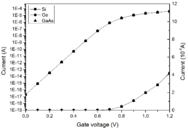
For the channel material simulation, we selected Si, Ge, GaAs as samples. However, the simulation
Figure 12. Wrong I-V characteristics from channel material simulations
result shown in Fig 12 implies that the channel material option in the simulator input deck did not work. All the drain current-gate voltage curves was almost exactly same to the 105th order. This result is wrong according to previous papers [4] To simulate various channel materials for NW, we tried to use manual material options. However, we could only set the longitudinal and transverse effective masses, channel bandgap, and channel dielectric constant. Since every material has a different affinity and different valley contribution, we cannot set a plausible input data for channel material dependence using only these options. To manage the inavailable channel material option, additional parameters such as band gap offset and different valley options, should be considered
CONCLUSION
In conclusion, we have shown that GAA Si N W MOSFET is the most adequate structure amo ng multigate FET structure for the sub 14nm tec hnology. Although it has superior performance f or short channel effects compared to other stru ctures, certain SCE still remains. However, the th e characteristics of GAA Si NW differs from the
traditional planar MOSFET due to quantum effec ts. These quantum effects were analysed by appl ying various variables in attempt to find the wa y to reduce SCE. It was observed that sub 10n m gate length exhibited dramitcal increase of S CE due to source-drain tunneling. Channel area under 2nm 2nm also showed sudden increase of SCE due to quantum confinement. Although not observed due to simulation limitations, reduction of oxide thickness results leakage current due to tunnelling. High K dieletrics induced fringing capacitance, introducing SCEs. Lastly, although available to the simulation but not operating properly, channel materials and their transport orientation governed the I-V characteristics by quantum confinement and valley splitting. Such phenomenons were observed by these various variables, and will be used for understanding the device charactersitics for future sub 14nm devices.
ACKNOWLEDGEMENT
This research was supported by the EDISON Program through the National Research Foundation of Korea(NRF) funded by the Ministry of Science, ICT & Future Planning (No. NRF-2012- M3C1A6035302)
We express special thanks to our adviser, Professor Seunghyup Yoo.
REFERENCES
[1] Anisur Rahman et al., Journal of Applied Physics.
97, 053702 (2005).
[2] Kelin J. Kuhn et al. "Considerations for Ultimate CMOS Scaling", IEEE Transactions on Electron Devices, 59, no.7 (2012)
[3] Saumitra Mehrotra
et al.
, “A Simulation Study of Silicon Nanowire Field Effect Transistors”,Universoty of Cincinnati (2007)
[4] The Channel Material Study of Double Gate Ultra-thin Body MOSFET for On-current Improvement, Journal of EDISON Nano-physics,
3, 60-62 (2014)
[5] Jing Wang
et al
., “Bandstructure and Orientation Effects in Ballistic Si and Ge Nanowire FETs”, Electron Devices Meeting (2005)73