An Advanced Embedded SRAM Cell with Expanded Read/Write Stability and Leakage Reduction
Yeonbae Chung
*Abstract
Data stability and leakage power dissipation have become a critical issue in scaled SRAM design. In this paper, an advanced 8T SRAM cell improving the read and write stability of data storage elements as well as reducing the leakage current in the idle mode is presented. During the read operation, the bit-cell keeps the noise-vulnerable data ‘low’ node voltage close to the ground level, and thus producing near-ideal voltage transfer characteristics essential for robust read functionality. In the write operation, a negative bias on the cell facilitates to change the contents of the bit. Unlike the conventional 6T cell, there is no conflicting read and write requirement on sizing the transistors. In the standby mode, the built-in stacked device in the 8T cell reduces the leakage current significantly. The 8T SRAM cell implemented in a 130 nm CMOS technology demonstrates almost 100 % higher read stability while bearing 20 % better write-ability at 1.2 V typical condition, and a reduction by 45 % in leakage power consumption compared to the standard 6T cell. The stability enhancement and leakage power reduction provided with the proposed bit-cell are confirmed under process, voltage and temperature variations.
Key words: SRAM, embedded memory, 8T cell, data stability, leakage current
* School of Electronics Engineering, Kyungpook National University
※
This research was supported by Kyungpook National University Research Fund, 2012. This research was also supported by Basic Science Research Program through the National Research Foundation of Korea (NRF) funded by the Ministry of Education, Science and Technology (2011-0003098). The CAD tool was supported by the IC Design Education Center.
Manuscript received Jul. 17, 2012; revised Sep. 26, 2012; accepted Sep. 26, 2012
I. Introduction
Technology scaling and increasing random variation in MOSFET characteristics reduce the operational margin of SRAM functionality. Most of current SRAM designs employ the 6-transistor (6T) memory bit-cell composed of two cross-coupled inverters with a set of access transistors. In this traditional 6T SRAM cell, the transistor strength ratios must be chosen such that the read static noise margin (SNM) and the write margin (WM) are both maintained, which presents conflicting constraints on the cell transistor strengths. This
delicate balance of transistor strength ratios can be severely impacted by device variation, which dramatically degrades the cell operating margin in scaled technologies. Low supply voltages further exacerbate the problem since the threshold voltage variation consumes a large fraction of these voltage margins.
To overcome this stability issue, many different structures of SRAM bit-cell have been explored.
For examples, the 7T cell [1] may improve the read
stability by cutting off a pull down path during
read operation. But it has a limited write capability
due to the single-ended write operation. The 8T
[2-4], 9T [5] or 10T [6, 7] SRAM cells decouple the
data storage elements and the data output elements,
and hence making the read SNM equal to the hold
mode SNM. Write-ability is equal to that of the 6T
cell. However, they do not have efficient
column-interleaving structure in the write operation,
which might be critical to cope with multi-bit
errors. They also might suffer an access time
degradation due to the single-ended read-bitline
structure [2-4, 6, 7]. A data-aware SRAM cell [8], which circumvents the column-interleaving issue in the write operation, consumes a substantial dynamic power because all the non-selected wordlines in the memory array should be toggled during each read and write access. Another 8T cell [9] achieves an exceptional improvement in the read stability, but there is a difficulty in the write operation for low supply voltage. The other cell options [10, 11] may increase the read stability, but they carry considerable area penalty in the cell size and hence making unacceptable for most applications.
In this work, improvements of the previous 8-transistor (8T) SRAM cell [9] are addressed. The proposed cell not only enhances the read stability, but also increases the write-ability of the cell inverter pair under voltage variations. It utilizes a differential swing in the read and write path. A column by column negative bias scheme leads to improve the write-ability. There is no column-interleaving issue in the write operation.
Furthermore, the bit-cell achieves a significant reduction of the standby current due to the stacked leakage path. All the results in this paper were obtained in a 130 nm generic CMOS technology.
Typical threshold voltages of NMOS and PMOS are 0.34 V and -0.34 V, respectively. The nominal supply voltage for this process is 1.2 V.
II. Proposed SRAM Bit-Cell Fig. 1(a) shows a standard 6T SRAM cell, where MN1 and MN2 are the drive, MP1 and MP2 are the load, and MN3 and MN4 are the access transistors, respectively. The fundamental stability issue of this 6T cell occurs during the read access.
For the read operation shown in Fig. 1(b), the wordline (WL) makes a transition from low to high while the bitline pairs (BL, /BL) are maintained high. The internal node of the cell that represents a zero gets upward through the access transistor due to voltage dividing effect across the access transistor and drive transistor. Moreover, the voltage transfer gain of the cell inverter is lowered due to the parallel connection of the access transistor and the load transistor. This severely deteriorates the cell immunity to the noise. If the
(a)
DN /DN
MP1
MN1 MN3
MN2 MP2
MN4
BL /BL
WL
(b)
0.01.2
Voltage (V)
1.6
0.8
0.4
Time DN (Low) /DN (High)
WL
VDD= 1.2 V
Fig. 1. Standard 6T SRAM cell: (a) schematic; (b) waveforms showing the internal voltage rising in the read operation. (WL: wordline, BL:
bitline, /BL: /bitline, DN: data-node, /DN:
/data-node)
‘low’ node voltage is higher than the logic threshold of the other cell inverter, the cell contents may be flipped, resulting in a read failure. For the read functionality, it is desirable to strengthen the drive transistors and weaken the access transistors.
Meanwhile, to achieve a proper write operation, an access transistor with strong driving capability and relatively weak load transistor are desired. A careful transistor sizing to ensure a balanced stability for read and write operation is required with right device size to minimize SRAM cell area.
The proposed 8T SRAM cell is shown in Fig.
2(a). In its structure, two PMOS transistors (MP3, MP4) called conducting transistor are added between the access transistor and the drive transistor. Their gates are controlled by a column-wise write-assist line (WAL). In the standby mode, WAL is kept to the ground such that the conducting transistors are normally in on-state. Two cross-coupled inverters (MP1-MN1, MP2-MN2) in the cell hold their bi-stable data. The read operation shown in Fig.
2(b) is basically same as that of the standard 6T
cell. Initially consider that DN = 0 and /DN = V
DD.
(a)
DN
/DN MP1
MN1 MN3
MN2 MP2
MN4
BL /BL
WL
MP3
WAL PN
MP4 /PN
(b)
0.01.2
Voltage (V)
1.6
0.8
0.4
Time DN (Low) /DN (High)
WL
VDD= 1.2 V
Fig. 2. Proposed 8T SRAM cell: (a) schematic; (b) voltage waveforms for the read operation. (WL:
wordline, BL: bitline, /BL: /bitline, WAL:
write-assist line, DN: data-node, /DN:
/data-node)
At onset of a read access, the bitline pairs are precharged to high, and the write-assist line is tied to the ground. When the wordline is going to high, the voltage dividing in series along access transistor (MN3), conducting transistor (MP3) and drive transistor (MN1) represses voltage rising of internal node DN representing a zero. That leads to increase the read stability drastically. This effect is primarily depending on the threshold voltage of conducting-PMOS transistor. In contrast to the 6T cell, the strength of pull-down drive transistor can be reduced in this 8T cell. In the write access, the WAL signal is changed to a negative voltage. For a successful write, the bit-cell becomes mono-stable, forcing the internal voltages to the correct values.
Initially assume that DN = V
DDand /DN = 0. In order to write a zero to the node DN, BL is set to
‘0’ and /BL to V
DD. When WL is going to high, the node PN makes a transition from V
DDto a zero.
Since the gates of conducting transistors are biased to a negative voltage, the node DN can be
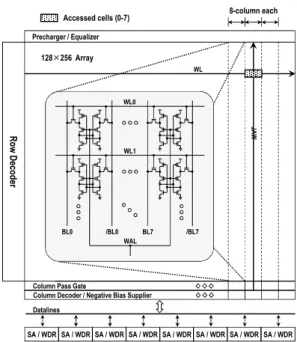
Row Decoder
Column Pass Gate
Column Decoder / Negative Bias Supplier Precharger / Equalizer
8-column each Accessed cells (0-7)
WL
Datalines
WAL
128Í256 Array
WL0
WL1
BL0 /BL0 BL7 /BL7
WAL
SA / WDR SA / WDR SA / WDR SA / WDR SA / WDR SA / WDR SA / WDR SA / WDR
Fig. 3. Configuration of 8T SRAM memory block. (SA:
sense amplifier, WDR: write driver)
discharged easily from V
DDto a zero state. Falling of the node DN brings the inverter MP2-MN2 to trigger. The positive feedback inside the cell changes the contents of the cell.
Fig. 3 shows an example of 32-kbit SRAM array incorporating the proposed 8T cell. The logical organization is basically same as that of the conventional 6T SRAM array. A unique feature is that the negative bias supplier controls the WAL signal running parallel to the bitlines and feeds eight WALs in common. The remaining core circuitry and peripheral logic are essentially same as those for conventional one. For each write cycle, a negative bias supplier decoded by column address activates only eight of interleaved columns. The cells from remaining columns on a selected row will experience a dummy read operation. Moreover, the un-accessed cells on the selected columns will be in the standby mode.
Fig. 4 shows a negative bias supplier and the
simulated waveforms associated with a write access
using this scheme. The circuit consists of column
decoding gates, capacitor driver, boosting capacitor,
negative level shifter and pre-bias transistor. A
M2 M1 PRE
Y
PB WAL
Negative level shifter
Capacitor
Pre-bias transistor Driver
Column decoding gates
A
D
B C
M4 M3
M5
(a)
-0.3 0.0 0.9 1.2
Voltage (V)
-0.6 1.5
0.6 0.3
-0.3 0.0 0.9 1.2
-0.6 1.5
0.6 0.3
Time (ns)
12 13 14 15 16 17 18
10 11
D A
C B
BL, /BL DN, /DN WL
BL, /BL
WAL
WL B D
A
(b)
Fig. 4. Negative bias supplier: (a) circuit configuration; (b) simulated waveforms in the write access at V
DD= 1.2 V.
triple-well technology is used for the separated-body NMOS transistors (M3, M4, M5). In the initial state, the input node A of negative level shifter and the node D of boosting capacitor are both in V
DDlevel. Transistors M2 and M3 are on, and M1 and M4 are off, holding the node C at V
DD. Thus WAL is connected to the ground by the pre-bias transistor M5. At the beginning of the write access, the column pre-decoded signal Y selects a proper local negative bias supplier. Then the preset signal PRE with high transition makes the node A the ground. M1 and M4 are on, and M2, M3 and M5 are off, allowing WAL to float.
The succeeding signal PB changes the node D to the ground, and thus WAL is boosted to a negative voltage V
WALby capacitive coupling. Next, the bitlines are driven with the new data. When the wordline is activated later on, the cell data nodes (DN, /DN) flip from one state to another
Table 1. Dimension of SRAM bit-cell transistors.
6T cell 8T cell
Width/Length (nm/nm)
Load transistor 150/130 150/130 Access
transistor 150/130 360/130 Conducting
transistor - 150/130
Drive
transistor 270/130 150/130
Beta ratio 1.8 0.42
immediately. After the wordline is switched again to the ground, the signals PB and PRE return both boosting capacitor and negative level shifter to the initial state. On the other hand, the V
WALlevel, determined by the ratio of boosting capacitor and parasitic capacitances associated to the WAL node, is -0.48 V at 1.2 V supply, that is, V
WAL= -0.4V
DDin this example. For the 130 nm CMOS technology used in this work, the gate oxide thickness is 30 Å, and the breakdown voltages for NMOS and PMOS are 2.5 V and -2.5 V respectively. Since the maximum stress voltage (here 1.68 V) on the transistors connected to the WAL node is relatively small, it would not affect the reliability of transistors.
III. Bit-Cell Performance and Discussions
3.1. Bit Area
For comparisons of stability and leakage properties, the 6T and proposed 8T cells have been implemented in a 130 nm generic CMOS technology.
The dimensions of each cell transistor are summarized in Table 1. In the standard 6T cell, the width of drive transistor is 270 nm while those of other transistors are 150 nm. The cell beta ratio, defined as the ratio of W/L for driver transistor to W/L for access transistor, is equal to 1.8.
The layouts of the 6T and 8T SRAM cells are
shown in Fig. 5. These layouts have been drawn in
a pure logic design rule without any cell-based
specific rule. In drawing the 8T cell, the PMOS and
drive transistors layout was first formed with the
minimum dimension of the design rules. The access
(a)
(b)
Fig. 5. SRAM cell layouts: (a) standard 6T cell (1.65×2.06 µm
2); (b) proposed 8T cell (1.65×2.85 µm
2).
transistor layout was then formed within tolerance of the cell area. The bitline contacts and conducting-PMOS gate contact are shared with neighboring cells. As the result, W/L of access transistor is 360/130 nm. The other transistors have a minimum device size. The 8T bit-cell adds 38 % area overhead relatively to the 6T cell. In more scaled CMOS technology such as 65 nm, 45 nm and beyond, the thin cell layout approach [12] might be effective to reduce the lithographic mismatch. But the area overhead may be remained in a same degree since both 6T and 8T cells will be scaled in asame way.
3.2. Read Stability
Fig. 6 shows the simulated butterfly curves for both standard 6T and proposed 8T SRAM cells.
The plotted data was obtained using a set of
VDN(V)
0.0 0.2 0.4 0.6 0.8 1.0 1.2 0.0
0.2 0.4 0.6 0.8 1.0 1.2
V/DN(V)
6T cell 8T cell
Fig. 6. Simulated butterfly curves at V
DD= 1.2 V.
(a)
6T, SF 8T, SF
6T, TT 8T, TT
6T, FS 8T, FS
Temperature (℃) -40 -20 0 20 40 60 80 100 0
200 300 400 500
Read SNM (mV)
100 600
(b)
0200 300 400 500
Read SNM (mV)
100
VDD(V)
0.8 0.9 1.0 1.1 1.2 1.3
6T, SF 8T, SF
6T, TT 8T, TT
6T, FS 8T, FS
Fig. 7. Read static noise margin: (a) at V
DD= 1.2 V; (b) at T = 100 ℃.
nominal parameters at 1.2 V and room temperature.
The static noise margin (SNM) is a side of the maximum square in the curve. In spite of a small beta ratio, the SNM of the proposed 8T cell is about 100 % larger than that of the standard 6T cell. This is because that the internal node rising
MP3
VDD GND
BL MP4 /BL
MP1 MP2 WAL
MN1 MN2
MN3 MN4
WL
Unit cell N-well P-well
N-well P-well Unit cell
VDD GND
MP1 MP2
MN1 MN2
MN3 MN4 /BL
BL WL
Wordline voltage (V) 0.0 0.2 0.4 0.6 0.8 1.0 1.2 0.0
0.2 0.4 0.6 0.8 1.0 1.2
Data node voltage (V)
6T cell 8T cell
DN /DN
WM WM
Fig. 8. Simulated write-ability at V
DD= 1.2 V and V
WAL= -0.48 V.
representing a zero is limited below V
DD- V
TN-
|V
TP|, where V
TNand V
TPare the threshold voltages of NMOS access transistor and PMOS conducting transistor, respectively. This gives near-ideal butterfly curve essential for robust SRAM bit-cell design.
Fig. 7 shows temperature and V
DDdependence on the read stability for different process corners.
Here, TT means typical-NMOS and typical-PMOS, FS means fast-NMOS and slow-PMOS, and SF means slow-NMOS and fast-PMOS, etc. In FS (low V
TNand high V
TP) corner, the logic threshold voltage of the cell inverter would be decreased and thus getting the read stability worse. Similarly for SF (high V
TNand low V
TP) corner, the logic threshold voltage would be increased, getting the read stability better. As the temperature is raised, the read SNM decreases monotonously. At 1.2 V and 100 ℃ worst temperature, the variation in the read SNM between extreme corners (SF, FS) is 63 mV in the 8T cell compared to 100 mV in the 6T cell, indicating better process variation tolerance.
3.3. Write-Ability
Write-ability of a bit-cell gives an indication of how easy or difficult it is to write to the cell. The write margin (WM) in this work defines the difference between V
DDand a wordline voltage needed to flip the cell content when the bitline pairs are set with V
DDand 0 V [13]. The larger the voltage difference, the easier it is to write to the cell.
(a)
6T, SF 8T, SF
6T, TT 8T, TT
6T, FS 8T, FS
300 400 600
Write margin (mV)
Temperature (℃)
-40 -20 20 40 80 100
500 700
0 60
(b)
6T, SF 8T, SF 6T, TT
8T, TT
6T, FS 8T, FS
100 300 500 600 800
Write margin (mV)
VDD(V)
0.8 0.9 1.0 1.1 1.2 1.3
200 400 700
Fig. 9. Write margin: (a) at V
DD= 1.2 V and V
WAL= -0.48 V; (b) at T = 100 ℃ and V
WAL= -0.4V
DD.
Fig. 8 shows the simulated write-ability at 1.2 V, TT and room temperature. The plot for 8T cell was obtained with a WAL bias V
WALof -0.48 V.
The WM values are 446 mV and 537 mV for 6T and proposed 8T cells, respectively. Unlike the 6T cell, the strength of access transistor can be increased in the 8T bit-cell within tolerance of bit area. Owing to the negatively-biased conducting transistor with a strong access transistor, the node storing ‘1’ in the 8T cell is flipped at a much lower WL voltage, giving a higher WM. Compared to the 6T cell, the 8T cell gives better read stability as
well as better write-ability.
Fig. 9 shows the write margin simulation results across temperature and for different supply voltages.
The write-ability is getting better at a high
temperature because the PMOS load transistor
weakens relatively to the NMOS access transistor
(a)
VDD(V)
0.8 0.9 1.0 1.1 1.2 1.3
6T, -40℃
10-12 10-11 10-10 10-9 10-8
8T, -40℃
6T, 25℃
8T, 25℃
6T, 100℃
8T, 100℃
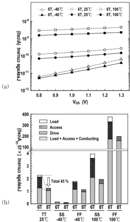
Leakage current (A/cell)
(b)
6T 8T 6T 8T 6T 8T 6T 8T 6T 8TLoad + Access + Conducting Access
Drive Load
0 2 4 100 300
Leakage current (×10-10A/cell) 1
25℃TT SS
-40℃ FF
-40℃ SS
100℃ FF
100℃
200 400
3
Total 45 %
Fig. 10. Standby cell leakage current: (a) at TT process corner; (b) at V
DD= 1.2 V.
as temperature rises. As V
DDincreases, the write margin also increases. A negative bias on the conducting transistor during write transition enables the 8T cell to achieve better write-ability in low supply voltage. As the result, the WM of 8T cell remains higher over the 6T cell across all of the voltage ranges. Moreover, the variation in WM across skewed process corners (FS, SF) at 1.2 V and -40 ℃ is 162 mV in the 8T cell compared to 201 mV in the 6T cell, showing better process
variation tolerance.
3.4. Leakage Power Consumption
The proposed bit-cell also lowers the total leakage power. For both 6T and 8T SRAM cells in the standby mode, the access transistors are cutoff and the bitline pairs are charged to V
DD. The gates
‘L’ ‘H’ ‘L’
PN /PN
‘H’