한국정보통신학회논문지 Vol. 23, No. 7: 822~828, Jul. 2019
증강현실을 위한 임베디드 시스템의 DMA 컨트롤러 설계
장수연1·오정환2·윤영현2·이성모2·이승은3*
Design of a DMA Controller for Augmented Reality in Embedded System
Su Yeon Jang
1· Jung Hwan Oh
2· Young Hyun Yoon
2· Seong Mo Lee
2· Seung Eun Lee
3*1
Undergraduate Student, Department of Electronic and Information Engineering, Seoul National University of Science and Technology, Seoul, 01811 Korea
2
Graduate Student, Department of Electronic Engineering, Seoul National University of Science and Technology, Seoul, 01811 Korea
3*
Associate Professor, Department of Electronic Engineering, Seoul National University of Science and Technology, Seoul, 01811 Korea
요 약
증강현실은 실제 환경과 함께 가상 정보를 제공하며, 이러한 시스템을 위해 프로세서의 메모리 접근이 요구된다.
하지만 기술 발전에 따라 데이터의 양이 증가함으로써, 프로세서의 작업량 또한 증가하게 된다. 이를 해결하기 위해 임베디드 프로세서의 작업 부하를 감소시킬 수 있는 특정 모듈을 필요로 한다. 본 논문에서는 임베디드 프로세서 대 신에 이미지를 출력하는 Direct Memory Acceass(DMA) 컨트롤러를 제안한다. 제안하는 DMA 컨트롤러를 Field Programmable Gate Array(FPGA)에 구현하고 Avalon Memory Mapped(Avalon-MM) 인터페이스를 기반으로 한 DMA 컨트롤러의 기능을 시연한다. 또한, DMA 컨트롤러를 Magnachip/Hynix 0.35um CMOS로 제작하고, 임베디 드 시스템의 실현 가능성을 검증한다.
ABSTRACT
An Augmented Reality(AR) provides virtual information with a real environment, and the processor needs to access the memory for the AR system. However, the processor has the heavy workload as the technology improvement leads to increase the size of data. We need a specific module to reduce the workload to overcome the limitation. In this paper, we propose a Direct Memory Access(DMA) controller displaying image instead of the processor. We implemented the proposed DMA controller on a Field Programmable Gate Array(FPGA) and demonstrated the functionality of the DMA controller based on an Avalon Memory Mapped(Avalon-MM) interface. Also, the DMA controller is fabricated by using Magnachip/Hynix 0.35um CMOS technology and verified the feasibility of the embedded system.
키워드
: 직접 메모리 접근, 임베디드 시스템, 증강현실, FPGA
Keywords
: Direct Memory Access, Embedded System, Augmented Reality, Field Programmable Gate Array
Received 20 May 2019, Revised 27 May 2019, Accepted 10 June 2019
* Corresponding Author Seung Eun Lee(E-mail:[email protected], Tel:+82-2-970-9021)
Associate Professor, Department of Electronic Engineering, Seoul National University of Science and Technology, Seoul, 01811 Korea Open Access
http://doi.org/10.6109/jkiice.2019.23.7.822
print ISSN: 2234-4772 online ISSN: 2288-4165with a real environment. The users get the extra information on a monitor in real time. By adopting the AR in daily life, the users enhance the efficiency of their work. In [1], the system with the AR helps a manager to manage a field by checking the virtual information of the field environment. In [2], a driver who drives a vehicle with the AR enables to check the helpful traffic information on the front window. The OVJET which is one of AR applications supplies social network service (SNS) and global positioning system (GPS) to offer various information to users of this application [3]. The AR requires comparison process of the image data from a camera with the pre-existing data in the memory and image processing process for displaying virtual information on a monitor. When the image data is matched to the pre-existing data in the memory, the processor provides the valid information which is blended in the image data for users. By applying this technology to the embedded system, people enable to utilize the AR in their lives.
However, the improvement of technology leads to increase the size of the image data from the camera due to high resolution. When the embedded processor processes the large amount of the image data and accesses memory in real time, the workload of processing degrades the performance of the entire system [4]. The processor disables to process other operations during displaying the image data. In order to improve the performance of the embedded processor, we need an extra specific module which reduces the workload of the processor. A direct memory access (DMA) controller enables to access memory and to make the processor do other operations. In [5], the DMA controller transfers massive data via the local bus and the multi-port memory controller. Also, Song’s study proposes the memory architecture for the DMA controller to access memory more efficiently [6]. An AMBA-based advanced DMA controller is designed for enhancing
rate. In order to make the processor work efficiently, the DMA controller displays the image data that requires a lot of memory access instead of the processor in the embedded system. Therefore, the processor enables to do the other operations while the image data is being displayed by the DMA controller.
In this paper, we propose a DMA controller displaying image data to reduce the workload of the processor in the embedded system with the AR. The proposed DMA controller communicates with the processor and the memory through an Avalon interface. Our design of the DMA controller accesses the memory to display the image data instead of the processor. The rest of this paper is organized as follows. In section Ⅱ, we introduce the architecture of the embedded system with the DMA controller and the architecture of the proposed DMA controller in detail. Section Ⅲ presents simulation results for verifying the functionality of the DMA controller. In section Ⅳ, we show the verification of a chip which is the DMA controller designed. Finally, we conclude the study in section Ⅴ.
Ⅱ. ARCHITECTURE OF SYSTEM AND DMA CONTROLLER
Fig. 1 illustrates the structure of the entire system. A camera sensor transfers image data of the real environment to the embedded processor. After the processor receives the image data from the camera sensor, the processor compares the image data to the pre-existing data in the memory. When the image data is matched, the processor mixes the information data from the memory and the image data from the camera sensor.
After processing these images, the processor accesses
the memory to save the augmented image data. In the
embedded system with the DMA controller, the processor
requests a displaying operation to the DMA controller.
The DMA controller sends a signal to the memory controller to access the image data. The DMA controller receives the image data from the memory to display. As the DMA controller displays the image data on a monitor instead of the processor, the processor enables to do other operations in that time. In this entire system, the image processing and the image displaying operations are separated to overcome the limitation in the embedded system.
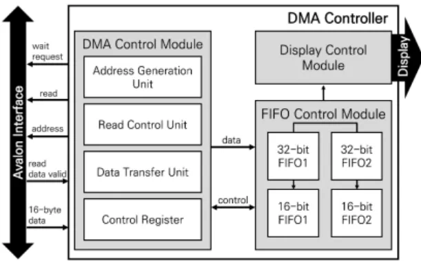
Fig. 2 illustrates the architecture of the DMA controller in the proposed embedded system. The DMA controller consists of a DMA control module, a FIFO control module, and a display control module. An Avalon Memory Mapped (Avalon-MM) interface is used to communicate signals or data among the processor, the DMA controller, and the SDRAM. The DMA controller is available to be set as a master or a slave in the Avalon-MM interface. When the DMA controller is a slave and the processor is a master, the master controls the operations of the DMA controller.
On the other hand, when the DMA controller is a master in the interface, the DMA controller directly accesses to the SDRAM. The DMA is supporting the Avalon-MM interface which allows to connect with the FPGA easily.
The Avalon-MM has the typical address interface for the connection between a master and a slave [9]. The Avalon interface fabric requires 32-bit because the width of the image data is 32-bit. The DMA controller is designed by the specification of the Avalon-MM interface.
Fig. 2 The architecture of the DMA controller
2.1. DMA Control Module
The DMA control module consists of an address generation unit, a read control unit, a data transfer unit, and a control register. This module generates a signal for preventing collisions and accessing memory such as read and wait_request signals. When a master reads the data, the address generation unit sends 1-byte applicable address to a slave. When the DMA controller reads 16-byte data from the SDRAM, the maximum value of burst count must be a power of 2 by the specifications of the Avalon interface. Also, the minimum burst count is one. The address generation unit controls the address according to the size of the image data and the number of frames in the control register. The read control unit allows the read signal to set high or low in accordance with the wait_request signal for preventing collisions among masters and slaves in the Avalon-MM interface.
In this system, the wait_request and the read signals are
active at high state. When the wait_request signal is high
state, the DMA controller as a master transfers the data
in the SDRAM through the Avalon-MM interface. On
the other hand, when the wait_request signal is low state,
the DMA controller as a slave is ready to respond the
read request of the processor as a master. The low of the
wait_request signal means the read control unit sends a
read request. As the result, the read signal is set by the
wait_request signal. When the DMA controller requests
to read the image data in the SDRAM, a read_data_valid
which is a 1-bit signal is asserted by the SDRAM. When
Fig. 1 The structure of the entire systemnumber of transfers in each burst. The burst count increases from 1 to 4 to transfer the 16-byte data and address increases by 16 because the Avalon-MM interface is required 32-bit. The data transfer unit controls to transfer the image data to one 32-bit FIFO in the FIFO control module. The control register includes information for start operation, the number of frames, the size of the image data, and the burst count.
2.2. FIFO Control Module
The FIFO control module is composed of two 32-bit FIFOs and two 16-bit FIFOs. Each size of two 32-bit FIFOs and two 16-bit FIFOs is 2048-byte. A set of FIFOs has a 32-bit FIFO and a 16-bit FIFO. In our design, the FIFO control module has two set of FIFOs to display the image data in real time. These two 32-bit FIFOs are used to receive the image data from the DMA control module turn by turn. These 32-bit FIFOs transfer the lower 16-bit image data to each 16-bit FIFO of the same set, after the higher 16-bit image data. These 16-bit FIFOs are used to transfer the image data to the display control module which is used to display the image data on a monitor. These two sets of FIFOs transfer the image data alternately to display control module in real time.
2.3. Display Control Module
The display control module supporting a RGB565 color format which represents 16-bit per pixel is necessary for displaying the image data received from the FIFO control module in real time. The RGB565 format consist of 5-bit red, 6-bit green, and 5-bit blue. In this design, the resolution of one frame is 640×480 and a row of one frame is 1280-byte. Also, the refresh rate is 60Hz. The display control module generates active signals such as horizontal sync and vertical sync signals. The horizontal sync signal is asserted to start another row of 640 pixels.
The vertical sync signal is asserted to start a new frame.
Ⅲ. SIMULATION RESULTS
We implemented the DMA controller and verified the functionality of the proposed DMA controller with simulations. In order to implement the DMA controller on an FPGA, we adopted DE2-115 development board including a SDRAM and a VGA connector for displaying on a monitor. We exploited Quartus Ⅱ 13.1 to synthesize the Avalon-MM interface including the DMA controller in environment based on the Avalon- MM interface fabric established by Qsys tool. First result is related to the wait_request signal. The wait_request signal is a necessary signal to avoid collisions between the master and the slave in the Avalon interface. Also, the wait_request signal is asserted by the slave when the slave is difficult to respond a read require from the master. Fig. 3 shows the simulation result of the wait_request signal when the burst count is four. When the system sets the wait_request signal low, the DMA control module requests a read operation to the SDRAM controller. On the other hand, when the SDRAM controller responds the read operation, the system sets the wait_request signal high. While the DMA controller is reading the 12-byte image data, the wait_request signal holds high state. In this time, the SDRAM controller is hard to respond another read operation.
After the last 4-byte is read by the DMA controller, the SDRAM controller sets the wait_request signal low.
Then the SDRAM controller enables to respond another
read operation from the DMA controller. Fig. 4 shows
wait state initialization of the SDRAM. When the
SDRAM controller responds the read operation, the
SDRAM initializes for implementing power-up sequence
and setting the mode register of the SDRAM by the
SDRAM controller. The SDRAM controller asserts the
wait_request signal to the Avalon-MM interface fabric
during initialization of the SDRAM. After initialization
of the SDRAM, the DMA control module enables to access 1280-byte of the image data. Fig. 5 shows output of the image data from the DMA control module. When the read_data_valid signal is set high state, the DMA control module transfers the image data to the FIFO control module. The source stream data signal presents the image data from the DMA control module to the FIFO control module. Fig. 6 shows the image data transmitted from the 16-bit FIFO to the display control module. When the horizontal sync signal is low state, the display control module displays the image data which is transmitted from the first 16-bit FIFO on a monitor. At this time, the second 16-bit FIFO receives the image data from the second 32-bit FIFO. After the display control module displays the image data, when the next horizontal sync signal is set high state, the second 16-bit FIFO reads the image data. By implementation of the DMA controller, we verified functionality of the proposed DMA controller.
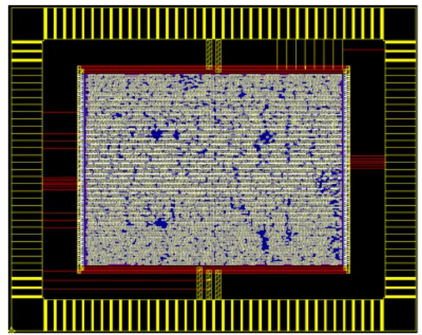
Ⅳ. CHIP IMPLEMENTATION AND VERIFICATION
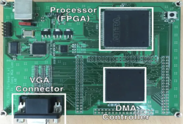
The DMA controller was fabricated by using Magnachip/Hynix 0.35um CMOS technology as shown in Fig. 7. Fig. 8 and Fig. 9 show the verification environment for the designed DMA controller, a VGA a
Fig. 3 The simulation result of the wait_request signalFig. 4 Wait state initialization of the SDRAM
Fig. 5 Output of the image data from the DMA Control module
Fig. 6 The system architecture of the DMA controller
Fig. 7 Layout of the DMA controller
which is a master on the Avalon-MM interface controls the DMA controller. Therefore, the JTAG-Avalon master bridge enables the image data in the SDRAM to be initialized by a System Console. The System Console provides read and write access to the IPs [10]. In order to verify the functionality of the proposed DMA controller, A procedure of the verification is as follows:
․The subsystem is set by the Qsys and the file is downloaded to the FPGA.
․The system console initializes the data of the SDRAM.
․We configure the control register of the DMA controller to start operation with the JTAG-Avalon master bridge.
Ⅴ. CONCLUSION
In this paper, we designed the DMA controller displaying image to reduce the workload of the processor in the embedded system with the AR. We used the SDRAM to save the image data and the SDRAM controller for initialization. The proposed DMA controller accesses the image data in the SDRAM memory for displaying instead of the processor to reduce the workload of the processor. By using Avalon interface, the DMA controller enables to communicate data between the processor and the SDRAM. We implemented the operations of the proposed DMA controller and fabricated it by using CMOS technology. Also, we verified the functionality of the DMA controller. For the future work, we plan to implement the performance of the system by using the other bus interface such as an AMBA instead of the Avalon-MM interface.
Fig. 8 The front of the proposed DMA controller
Fig. 9 The back of the proposed DMA controller
ACKNOWLEDGEMENT
This study was supported by the Research Program funded by the Seoul National University of Science and Technology (2018-0099).
REFERENCES
[ 1 ] H. S. Kim, C. Y. Kim, and I. G. Lee, “Implementaion of sluice valve management system using GPS and AR,”
Journal of the Korea Institute of Information and Communication Engineering, vol. 21, no. 1, pp. 151-156, Jan. 2017.
[ 2 ] M. Choi, J. Lee, H. Jung, I. R. Tayibnapis, and S. Kown,
“Simulation framework for improved UI/UX of ST-HUD display,” IEEE International Conference on Consumer
Electronics (ICCE), Las Vegas, NV, pp. 1-4, 2018.
[ 3 ] B. H. Kim, “A Contest-award Mobile Augmented Reality Platform,” Journal of the Korea Institute of Information and Communication Engineering, vol. 16, no. 1, pp. 205-211, Jan. 2012.
[ 4 ] S. M. Lee, J. H. Jang, S. M. Lee, J. H. Oh, and S. E. Lee,
“Design of a DMA controller for loss-less image processing,”
IDEC Journal of Integrated Circuits and Systems, vol. 2, no.
2, Jun. 2016.
[ 5 ] F. Shanehsazzadeh, and M. S. Sadri, “Area and performance evaluation of central DMA controller in Xilinx embedded FPGA designs,” Iranian Conference on Electrical Engineering (ICEE), Tehran, pp. 546-550, 2017.
[ 6 ] I. K. Song, “A Design of Direct Memory Access (DMA) Controller for H.246 Encoder,” IEEE 8th International Conference on ASIC, Changsha, Hunan, pp. 419-422, 2009.
[ 7 ] G. Ma, and H. He, “Design and implementation of an advanced DMA controller on AMBA-based SoC,” Iranian Conference on Electrical Engineering (ICEE), Tehran, pp.
546-550, 2017.
[ 8 ] N. Nandan, “High performance DMA controller for ultra HDTV video codecs,” IEEE International Conference on Consumer Electronics (ICCE), Las Vegas, NV, pp. 65-66, 2014.
[ 9 ] Intel Corporation. Avalon Interface Specifications [Online].
Available: https://www.intel.com/content/dam/www/programmable /us/en/pdfs/literature/manual/mnl_avalon_spec.pdf.
[10] Altera Corporation . System Console User Guide [Online].
Available: https://www.intel.co.jp/content/dam/altera-www/
global/ja_JP/pdfs/literature/ug/ug_system_console.pdf.
장수연(Su Yeon Jang)
2015년 3월 – 현재 : 서울과학기술대학교 전자IT 미디어공학과 학사
※관심분야 : Computer architecture, system-on-chip design
오정환(Jung Hwan Oh)
2013년 3월 : 서울과학기술대학교 전자IT미디어 공학과 학사
2019년 2월 : 서울과학기술대학교 전자공학과 석사
※관심분야 : Computer architecture, system-on-chip design, and hardware multi-core scheduler design
윤영현(Young Hyun Yoon)
2013년 3월 : 서울과학기술대학교 전자IT미디어 공학과 학사
2019년 3월 – 현재 : 서울과학기술대학교 전자공학과 석사
※관심분야 : Computer architecture, m icroprocessor system, and system-on-chip design for machine learning
이성모(Seong Mo Lee)
2014년 2월 : 서울과학기술대학교 전자IT미디어 공학과 학사
2016년 2월 : 서울과학기술대학교 전자공학과 석사
※관심분야 : Computer architecture, system-on-chip design, and fault tolerant system design
이승은(Seung Eun Lee)
1998년 : KAIST, Bachelor of Science in Electrical Engineering
2000년 : KAIST, Master of Science in Electrical Engineering and Computer Science 2008년 : University of California, Irvine, Doctor
of Philosophy in Electrical and Computer Engineering
2009년 3월 – 2010년 8월 : Platform Architect, SoC Platforms Architecture Lab., Intel Labs., US
2010년 9월 – 2016년 9월 : 서울과학기술대학교 전자공학과 조교수
2016년 10월 – 현재 : 서울과학기술대학교 전자공학과 부교수
※관심분야 : Computer architecture, multi- processor system-on-chip design, low-power and resilient VLSI, and hardware acceleration for emerging applications