• 검색 결과가 없습니다.

Power Distribution Network Modeling using Block-based Approach

N/A
N/A
Protected

Academic year: 2021

Share "Power Distribution Network Modeling using Block-based Approach"

Copied!
5
0
0

로드 중.... (전체 텍스트 보기)

전체 글

(1)

Abstract: A power distribution network (PDN) is a network that provides connection between the voltage source supply and the power/ground terminals of a microprocessor chip. It consists of a voltage regulator module, a printed circuit board, a package substrate, a microprocessor chip as well as decoupling capacitors. For power integrity analysis, the board and package layouts have to be transformed into an electrical network of resistor, inductor and capacitor components which may be expressed using the S-parameters models. This modeling process generally takes from several hours up to a few days for a complete board or package layout. When the board and package layouts change, they need to be re-extracted and the S-parameters models also need to be re-generated for power integrity assessment. This not only consumes a lot of resources such as time and manpower, the task of PDN modeling is also tedious and mundane. In this paper, a block- based PDN modeling is proposed. Here, the board or package layout is partitioned into sub-blocks and each of them is modeled independently. In the event of a change in power rails routing, only the affected sub-blocks will be reextracted and re-modeled. Simulation results show that the proposed block-based PDN modeling not only can save at least 75%

of processing time but it can, at the same time, keep the modeling accuracy on par with the traditional PDN modeling methodology.

Keywords: BLock-based Modeling, Impedance Profile, Power Distribution Network, Power Integrity

1. Introduction

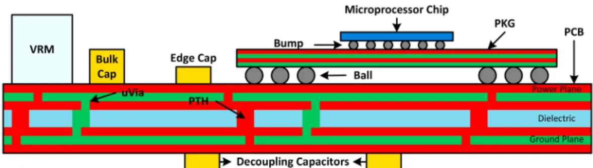
The power distribution network (PDN) comprises all the electrical and physical elements that form the electrical interconnects between the voltage source supply and the individual input/output buffers in a microprocessor chip. As shown in Figure 1, a typical PDN consists of a voltage regulator module (VRM), a printed circuit board (PCB), a package substrate (PKG) where the micro-vias and plated through holes are used to connect the different power and ground planes together, a microprocessor module as well as decoupling capacitors.

1-2)

In an electronic system, current that flows through the PCB and PKG from the VRM to the microprocessor chip creates a fluctuated voltage which is time-varying across the power and ground terminals of the chip. This not only affects the quality and stability of the voltage supply, it also affects the performance of the microprocessor in terms of operating frequency as well as power consumption. Thus, it is very important that a power integrity analysis be carried out to ensure that the designed PDN provides a well regulated voltage for the required current to be supplied to

the microprocessor over a specified time period.

1-5)

For a power integrity analysis, the PCB and PKG layouts first need to be extracted and transformed into an electrical network of resistor, inductor and capacitor (RLC) components which is called the S-parameters models. The Simulation Program with Integrated Circuit Emphasis (SPICE)

5)

analysis is then carried out to study the impedance profile and transient performance of the PDN.

The process of S-parameter modeling can generally take from several hours up to a few days for a complete PCB or PKG layout. When the PCB and PKG layouts change, they need to be reextracted and the S-parameters models also need to be re-generated for power integrity assessment.

5)

Hence, during the pre-maturity stages of a layout routing where power rails routing are often revised iteratively for an improved power integrity solution, it is necessary for the process of layout extraction, layout modeling and power integrity assessment to be repeated frequently. This is a waste of resources such as manpower and time. Besides, the task of PDN modeling is also tedious and mundane. In this paper, a block-based PDN modeling is proposed. Here, a PCB or PKG layout of W ×D×H dimension is first

Corresponding author

E-mail: [email protected]

© 2013, The Korean Microelectronics and Packaging Society

This is an Open-Access article distributed under the terms of the Creative Commons Attribution Non-Commercial License(http://creativecommons.org/

licenses/by-nc/3.0) which permits unrestricted non-commercial use, distribution, and reproduction in any medium, provided the original work is

properly cited.

(2)

partitioned into W/K×D/K×H blocks where K = {2, 3, 4 and etc.}. Each of these layout sub-blocks is then modeled independently. Should there be a subsequent change in power rails routing, only the affected subblocks will be re- extracted and re-modeled.

Using the proposed block-based modeling approach, it is shown that the simulation time of PDN modeling can be significantly reduced without sacrificing the performance of the existing power integrity solution. The remaining of this paper is organized as follows. Section 2 describes the evaluation process of a PDN design followed by a discussion of the proposed blockbased modeling approach in Section 3.

The simulation results and discussion are presented in Section 4 and finally, Section 5 concludes this paper.

2. Evaluation of Power Distribution Network Design

In a PDN, the VRM is the main power supply to the electronic system. Electric signals and power are routed from the board to the package through ball grid array joints.

These electrical signals and power are then distributed in the package substrate and are subsequently routed to the microprocessor chip through the controlled collapse chip connections. In general, the PDN shown in Figure 1 can be represented by distributed equivalent models of resistors, inductors and capacitors as shown in Figure 2.

Here, the bulk capacitor is modeled as an equivalent lumped circuit of a resistor, an inductor and a capacitor (R1, L1, C1) of 6 m Ω, 1.8 nH and 330 uF respectively. The PDN models (R2, L2) and (R3, L3) are the Sparameter models of the PCB and PKG respectively. All these resistance and inductance are contributed by interconnects as well as electrical parasitic on each of the system components. In addition, board decoupling capacitor (C2) of 22uF and the package decoupling capacitor (C3) of 1uF are assumed. It should be noted that this circuit will be used in the simulation presented in Section 4.

In a real world, current that flows through the PCB and PKG from the VRM to the microprocessor chip creates both a direct current drop and time-varying fluctuation of the voltage across the power and ground terminals of the chip.

This will greatly affect the performance of the microprocessor as the large voltage fluctuation across power and ground terminals can potentially impact the transistor's switching frequency which can cause timing margin errors. Besides, the increase in voltage across the power/ground terminals induces risk of transistor reliability issues. In view of this, it is very important that a power integrity analysis be carried out to ensure that the designed PDN provides a well regulated voltage for the required current to be supplied to the microprocessor over a specified time period.

1-5)

Figure 3 shows the process flow of how a PDN is being evaluated in most microelectronic designs. Firstly, the power Fig. 1. Cross sectional representation of a typical power distribution network.

Fig. 2. Distributed equivalent model of a power distribution network.

(3)

rails that are to be evaluated are extracted from the .brd and .mcm files for PCB and PKG design respectively using the SPDLinks software. The extracted .spd files are then fed into a commercial simulation tool such as Sigrity's PowerSI or Ansoft's SiWave for the PCB and PKG model extraction.

From a high level point of view, these tools use internal

used to generate the impedance and transient noise profiles of the designed system where they are in the frequency and time domains respectively. Analysis in the frequency domain enables the PDN designer to understand all the resonances and anti-resonances in the system produced by the interaction of inductances and capacitances in the PDN.

On the other hand, the time domain analysis allows the designer to evaluate the response of switching circuits in the PDN from the transient noise voltages generated across two nodes in the system.

6-8)

3. Block-based Modeling

Traditionally, when the PCB or PKG layout changes, the new layout needs to be re-extracted and the Sparameters file also needs to be re-generated for power integrity assessment.

This process can take as long as several days for a complete PCB or PKG layout modeling. In addition, during the pre- maturity stages of a layout where power rails routing are Fig. 3. Evaluation flow chart of power distribution network.

Fig. 4. Power distribution network modeling using block-based approach.

(4)

often revised iteratively for a better power integrity solution, this process of layout extraction, layout modeling and power integrity assessment has to be repeated frequently. This is time consuming and a waste of valuable manpower.

Furthermore, the task of PDN modeling is also tedious and mundane.

In view of this, a block-based PDN modeling approach is proposed. Here, a PCB or PKG layout of W×D×H dimension is first partitioned into W/K ×D/K×H subblocks as shown in Figure 4 where K = {2, 3, 4 and etc.}. Each of the layout sub-blocks are then fed into Sigrity's PowerSI or Ansoft's SiWave for model extraction. Here, connection ports are made at the edges of the layout sub-blocks as shown in Figure 4 so that they are able to be linked together during the SPICE simulation stage to form a complete PDN model. Figure 5 shows an example of SPICE simulation scripts used for PDN modeling using the proposed work. It can be seen that the S-parameters models of each layout sub-blocks are linked together by resistors of 100 uΩ.

The proposed block-based approach has the key advantage in that it can speed up the modeling time of a PDN significantly. In the event of a change in power rails routing or vias and PTHs connections are added or removed, only the affected sub-blocks are required to be re-extracted and re- modeled since each of the layout sub-blocks is modeled independently. This is extremely beneficial especially during the power routing performance investigation and debugging stages where layout changes are common.

4. Simulation Results anD Discussion

In this study, a PCB layout of dimension 64 mm×94 mm

×1.6 mm is used. It contains two power rails routing and

one ground plane. The PDN circuit diagram shown in Figure 2 is connected using the SPICE scripts presented in Figure 5. In these simulations, three PDNs are modeled: one with full layout extraction (K=1) and two with the full layout partitioned into four (K=2) sub-blocks and nine (K=3) sub-blocks for the proposed block-based modeling.

Impedance values are then measured at each of the power rails for each PDN model.

Figure 6 shows the impedance profiles comparison at power rails no. 1 and no. 2 for the three PDN models. From the simulation results, it can be seen that the proposed block-based PDN modeling gives a comparable impedance plot to the PDN modeling using a full layout extraction. For the worst case scenario, the resonance peak is shifted by 0.48 MHz and the amplitude delta is only 23 mΩ.

In Table 1, the PDN modeling speeds are recorded. Here, only one layout sub-block is assumed to have changes at any one time and the power routing complexity is also assumed to be about the same for each layout sub-blocks.

As anticipated, the proposed work can improve the modeling time of a PDN by a ratio of approximately K2.

Furthermore, by eliminating the tedious tasks such as full layout re-extraction and re-modeling, the power integrity engineers can benefit from a more constructive and beneficial work experience.

Fig. 5. SPICE simulation scripts for block-based modeling.

Table 1. Power distribution network modeling time for K = {1, 2, 3} when one of the layout sub-block is modified.

PDN Modeling Method Modeling Time

Full layout (K=1) 34.2 mins

4 Layout sub-blocks (K = 2) 8.7 mins

9 Layout sub-blocks (K = 3) 3.5 mins

(5)

Finally, it should be noted that there is an on-going research work to define a tuning module aimed at improving the correlation of PDN models using a full layout extraction and the proposed work. This tuning module will be located in between the layout submodels' connection ports. With tuning, it aims to provide an almost identical impedance plot for PDN modeling using the proposed block-based approach and the one using a full layout extraction.

5. Conclusion

This paper proposed a block-based PDN modeling approach where the board or package layout is partitioned into K2 sub-blocks and each of them is modeled independently. If there is a subsequent change in power rails routing, only the affected sub-blocks will be re-extracted and re-modeled. Simulation results show that the proposed block-based PDN modeling can improve the processing time by a ratio of K2 and at the same time, keep the modeling accuracy on par with the traditional PDN modeling methodology using a full layout extraction.

References

1. M. Swaminathan, E. Engin, “Power Integrity Modeling and

Design for Semiconductors and Systems”, Ed. 1, Prentice Hall Modern Semiconductor Design Series, Nov., (2007).

2. C. Wang and etc., “An Efficient Approach for Power Delivery Network Design With Closed-Form Expressions for Parasitic Interconnect Inductances”, IEEE Transactions on Advanced Packaging, May, 29(2), (2006).

3. B. Amelifard, M. Pedram, “Design of an efficient power delivery network in an soc to enable dynamic power man- agement”, ACM/IEEE International Symposium on Low Power Electronics and Design, Aug., 328, (2007).

4. L. W. Chew, “Design and Analysis of Power Delivery Net- work in a SoC: A Review”, Proceeding of International Con- ference on Electronics Packaging, ICEP, Apr., (2012).

5. Synopsys - SPICE Simulation Tool. http://www.synop- sys.com/Tools/Verification/AMSVerification/CircuitSimula- tion/HSPICE/Pages/default.aspx. Last accessed: Feb. (2013).

6. M. Popovich and E. G. Friedman, “Noise coupling in multi- voltage power distribution systems with decoupling capaci- tors”, Proc. IEEE Int. Symp. Circuits Syst., I, 620, (2005).

7. J. L Knighten, B. Archambeault, J. Fan, et al., “PDN Design Strategies: I. Ceramic SMT Decoupling Capacitors ? What Values Should I Choose?”, IEEE EMC Society Newsletter, Fall., 34 (2005).

8. L. W. Chew, “The Effect of Higher Order Model Decoupling Capacitors in the Design of a Power Delivery Network”, Pro- ceeding of 4th Asia Symposium on Quality Electronic Design, ASQED, Jul., 117, (2012).

Fig. 6. Impedance profiles comparison for layout extraction with K = {1, 2, 3}.

수치

Figure 3 shows the process flow of how a PDN is being evaluated in most microelectronic designs
Fig. 4.  Power distribution network modeling using block-based approach.
Figure 6 shows the impedance profiles comparison at power rails no. 1 and no. 2 for the three PDN models
Fig. 6. Impedance profiles comparison for layout extraction with K = {1, 2, 3}.

참조

관련 문서