저작자표시-비영리-변경금지 2.0 대한민국 이용자는 아래의 조건을 따르는 경우에 한하여 자유롭게 l 이 저작물을 복제, 배포, 전송, 전시, 공연 및 방송할 수 있습니다. 다음과 같은 조건을 따라야 합니다: l 귀하는, 이 저작물의 재이용이나 배포의 경우, 이 저작물에 적용된 이용허락조건 을 명확하게 나타내어야 합니다. l 저작권자로부터 별도의 허가를 받으면 이러한 조건들은 적용되지 않습니다. 저작권법에 따른 이용자의 권리는 위의 내용에 의하여 영향을 받지 않습니다. 이것은 이용허락규약(Legal Code)을 이해하기 쉽게 요약한 것입니다. Disclaimer 저작자표시. 귀하는 원저작자를 표시하여야 합니다. 비영리. 귀하는 이 저작물을 영리 목적으로 이용할 수 없습니다. 변경금지. 귀하는 이 저작물을 개작, 변형 또는 가공할 수 없습니다.
A THESIS FOR THE DEGREE OF DOCTOR OF PHILOSOPHY
Growth of nanostructured thin films for enhancing surface and
barrier properties using Roll-to-Roll chemical and atomic layer
deposition techniques
Srikanth Jagadeesan
Department of Advanced Convergence Technology and Science
GRADUATE SCHOOL
JEJU NATIONAL UNIVERSITY
REPUBLIC OF KOREA
Growth of nanostructured thin films for enhancing surface and
barrier properties using Roll-to-Roll chemical and atomic layer
deposition techniques
Srikanth Jagadeesan
(Supervised by Professor Kyung Hyun Choi)
A thesis submitted in partial fulfillment of the requirement for the degree of Doctor of Philosophy 2018.02
The thesis examined and approved
Thesis Director, Jong-Hwan Lim, Professor, Department of Mechatronics Engineering
Thesis Supervisor Kyung Hyun Choi, Professor, Department of Mechatronics Engineering
Yang-Hoi Doh, Professor, Department of Electronic Engineering
Chang-Nam Kang, Professor, Department of Mechanical Engineering
Jeong-Dai Jo, Principal Researcher, Korea Institute of Machinery & Materials ...
Date Department of Advanced Convergence Technology and Science
GRADUATE SCHOOL JEJU NATIONAL UNIVERSITY
Acknowledgments
I am extremely thankful to Jesus Christ for blessing me with the honor of achieving this task successfully. It was very long and tough journey, but He always guided me in the right direction. It was never an easy task, there were challenges, failures, sickness and many other problems but He kept me hopeful, confident, strong and helped me to sail my ship towards the shore. I would pray to Him that He would make me able to utilize my knowledge and education for the betterment of humanity.
I consider myself a very lucky person as I have been blessed with family especially my wife who has always been supporting me in my struggles. I extend my gratitude to Dr. Melvin David and family for their kindness and affection towards me. They are the ones who exposed me to the environment of higher education and were always there to watch my back.
I am extremely thankful to Prof. Kyung Hyun Choi who as a Ph.D. supervisor provided me with every possible opportunity to accomplish my goals. I will always be thankful and indebted to him for his kindness, support, trust, and motivation. I am also thankful to Kovindan who has been my teacher since my childhood. What I am today is because of the fact that my base was built on strong academic concepts by him.
I am thankful to those who helped me as my friends as well as mentors including Dr. Kamran Ali, Dr. Ghayas Uddin Siddiqui Dr. Navaneethan Duraisamy, Dr.Junaid, Dr.Shahid. I am thankful to my lab mates which include Memoon Sajid, Shahid Aziz, Muhammad Muqeet Rahman,Mutee Ur Rahman, Jahanzeb Gul, Imran Shah, Mushin Ali, Asad, Hyun Woo Dang, Bong Su Yang, Young Jin Yang, Go-Bum Kim, Hyeon Beom Kim, Soo Wan Kim, and Young Soo Kim. I am greatly thankful to all my friends particularly MSP Sudhakaran, Parthiban, Ganeshkumar, Premkumar,Vimal for providing homely environment during my long stay at Jeju.
Finally and most importantly, I would like to thank the gentlest and kindest peace of my heart whose presence is a real treasure and has always been acting as a driving energy for me towards greater successes. May God always keep my peace of heart strong and cherished so that I can keep hoping, and living strong and confident.
Contents
List of figures...iv
List of Tables...iv
Abstract...X CHAPTER-1 1. Introduction...1
1.1. Back ground of barrier coatings... 1
1.1.1. Permeation Mechanism...2
1.1.2. Current barrier layer development...3
1.2. Thin film techniques for barrier coatings... 4
1.2.1. Plating.... 5
1.2.2. Sol-gel...6
1.2.3. Chemical vapor Deposition...7
1.2.4. Atomic Layer Deposition...7
1.3. Spatial atomic layer deposition...9
1.4. Roll-to-Roll spatial Chemical &Atomic Layer Deposition...10
1.5. Inorganic Transparent barrier coating on the polymers...11
1.6. Scope of the current research... 14
CHAPTER-2 2. Experimental procedure ... 15
2.1. Materials and Method ... 15
2.2. Roll- to-Roll atmospheric chemical vapor deposition TiO2... 16
2.3. Al2O3deposited On PET substrate through R2R-AALD... 18
2.4. R2R-AALD SiO2thin film On PET substrate... 21
2.5. PVDF depositing through EHDA technique... 22
2.6. Multilayer thin film preparation... 24
2.7. Thin film characterizations... 25
CHAPTER-3 3. Results and Discussion ... 26
3.1. Low temperature deposited TiO2 Thin Films ... 26
3.1.1. Film Growth ... 28
3.1.2. Surface Morphology ... 30
3.1.3. Optical transmittance ... ... 33
3.1.4. Compositional analysis ... 34
3.1.5. Electrical properties ... .. 36
3.2. Single layer Al2O3deposited on PET substrate ... . 37
3.2.3. compositional Analysis...41
3.2.4. Barrier properties...42
3.3. Hybrid multilayer barrier coating...43
3.3.1. Surface morphology...46 3.3.2. Compositional analysis...48 3.3.3. Optical transmittance...50 3.3.4. Barrier properties...51 3.3.5. Mechanical properties...52 CHAPTER-4 4. Conclusions and Future Work...54
List of figures
Figure.1.1. Example of flexible electronics devices: (a) Flexible organic solar cell (b) Flexible LCD (c) Samsungs's OLED...1
Figure. 1.2. Thin film deposition techniques...5 Figure.1.3 Schematic of SALD reactor concept showing continuous flow of precursors, inert gas, and film deposition over movable substrate...10 Figure.1.4.The R2R deposition system: (a) R2R-CVD, (b) R2R-ALD...11
Figure.2.1. Schematic diagram of roll to roll atmospheric chemical vapor deposition...18 Figure.2.2. FESEM images of TiO2thin film on PET substrate. (a)Room temperature slow
decomposition nonuniform TiO2thin film, (b) Uniform TiO2thin film deposited at 100º C...19
Figure.2.3. Schematic diagram of the roll to roll atmospheric atomic layer deposition...20 Figure.2.4. The Photographic illustration of the roll to roll atmospheric atomic layer deposition and with their component's information...21
Figure.2.5. Optical image representation of the electrohydrodynamic atomization system for thin film deposition experiment...23 Figure.2.6. Schematic illustration of the multilayer barrier film preparation as well as thickness of each film...24
Figure .3.1.The deposition rate (nm/min) of the TiO2thin film increased while increasing the temperatures such as RT, 50, 75 and 100 °C...28
Figure.3.2. FESEM images of TiO2thin film on PET substrate. Nonuniform TiO2thin film
deposited at (a) RT, (b) 50 °C and uniform TiO2thin film deposited at (c) 75 °C, (d)
film at (c) 75 °C and (d) 100 °C...32
Figure 3.4. Optical property of TiO2thin film on the PET substrate by R2R-ACVD at room temperature to 100 °C. The optical transmittance was observed at 91 % in the visible region for 100 °C...34
Figure.3.5. The XPS spectra of R2R-ACVD TiO2films deposited at different temperatures (a) O 1s and (b) Ti 2p from TiO2films...36
Figure.3.6. The I-V characteristics of TiO2film at RT to 100 °C temperature grown on PET substrate...37 Figure 3.7 Thickness of deposited Al2O3films on PET substrates versus the number of process
cycles at 50 °C under the web velocity of 7mm/second (a), and growth rates of the Al2O3films
versus the web velocity (b)...40
Figure 3.8.FESEM images of the bare PEN substrate (a), Al2O3-coated PET at 50 °C (b), and 2D surface profile of the Al2O3films grown at 50 °(c)...41
Figure 3.9. The XPS spectrum of Al2O3film deposited at 50 °C...42
Figure.3.10. The WVTR and OTR values of the 50 °C deposited single layer Al2O3via R2R-AALD...43
Figure.3.11. The FESEM image of (a) R2R-AALD coated SiO2 thin film, (b) EHDA deposited PVDF, (c) 2D surface profile of the R2R-AALD SiO2 thin film (d) EHDA deposited PVDF (e) Contact angle of the R2R-AALD coated SiO2 (f) PVDF...47
Figure.3.12. The FIB cross-sectional image illustrating the thickness of the each layer...48
Figure.3.13. XPS spectrum of the multilayer barrier thin film: (a) R2R-AALD SiO2thin film (b) EHDA deposited PVDF thin film , (c) Hybrid PVDF/SiO2barrier thin film...49
Figure.3.15. The WVTR values of the single and multilayer barrier thin film depending on the
film thickness. The image shows that the decrease in WVTR value increases the film
thickness...51 Figure.3.16. The schematic illustration of the multilayer barrier thin film working mechanism in the atmospheric molecules...52
Figure.3.17. The water vapor transmission rate (WVTR) of the multilayer barrier film before and after bending test...53
List of Tables
Table. 2.3: The operational parameters of R2R-AALD system...20 Table. 3. 1: Summary of the growth rate observed in the Previous Reports...29 Table. 3.2: Atomic Composition of TiO2 film prepared by R2R-ACVD with different substrate temperature...35
ABSTRACT
In recent days flexible devices have begun to be regularly used in our daily lives for communications, renewable energy resources, and information technology. Conventional glass substrates can provide excellent protection from permeation species, but the glass substrate is rigid due to which it cannot be used for the application of flexible electronics. On the other hand, electronic devices made on flexible plastic substrates such as, organic thin film transistors (OTFTs), solar cells , and organic light emitting diodes (OLEDs) enable low cost, flexible, mass production and weight reduction in these devices. However, flexible polymer substrates can be easily damaged
by the atmospheric gas molecules oxygen (O2) and water (H2O) and therefore these substrates must
be protected with some additional encapsulating nanolayer. Several deposition techniques have been reported for the successful development of encapsulating thin films in order to protect electronic devices. These fabrication techniques include sputtering, thermal evaporation with good surface and barrier properties. However, these methods are only suitable for vacuum coating and rigid device coatings and cannot meet the requirements of atmospheric condition fabrication. Hence the researcher moved to the under atmospheric condition high quality thin film fabrication for flexible electronics applications.Among the variety of thin film process atmospheric roll to roll chemical and atomic layer deposition process have highly contributed thin film industry for mass production.
This thesis report to the inoroganic TiO2and Al2O3 thin film deposited on a flexible PET substrate
by using atmospheric roll-to-roll chemical and atomic layer deposition. The R2R-ACVD deposited
(100° C) TiO2 thin film expressed excellent surface,chemical,optical and electrical properties. The
developed single layer Al2O3 thin film also exhibited excellent surface,chemical and better barrier
properties.
Finally, a multilayer barrier thin film based on polyvinylidene difluoride (PVDF) –silicon dioxide
(SiO2) has been fabricated on the PET substrate through a novel method of joint fabrication
techniques. The Inorganic SiO2 thin film was deposited using a roll to roll atmospheric atomic
layerdeposition system (R2R-AALD) while the organic PVDF layer was deposited on the surface of SiO2 through Electro hydrodynamic atomization (EHDA) techniques. The multilayer barrier thin films exhibited very good surface morphology, chemical composition and optical properties. The total thickness of the multilayer barrier thin film was 520 nm with a high optical transmittance value (85-90%). The obtained value of water vapor transmission rate (WVTR) of the barrier thin film was
~ 0.9 × 10⁻² g m-2 day-1. This combination of dual fabrication techniques R2R-AALD and EHDA
CHAPTER 1
1. Introduction
1.1. Background of barrier coating:
In recent years flexible electronic highly occupied in our daily life in information technology, communications, renewable energy resources. Conventional glass substrate provides supreme, quality of protection from environmental species, but the glass substrates are rigid and brittle nature, therefore which cannot be used in an application of flexible electronics. But many of the research focus to fabricate the electronic device on plastic substrates such as organic solar cell, organic light emitting diode, Flexible liquid crystal display showed in Figure.1.1.The main reason for such organic device arises due to their multifunctional characteristics, tunable properties and high potential use in flexible electronics.[1-5] However, the major disadvantage of this flexible electronics can easily oxidized and damage electrodes by water vapor or oxygen from the ambient environment. Thus the lifespan of organic electronics is the major concern to produce who need to ensure at any rate up to around 20000 hours of continuous use.Upcoming years expected to increase by 50-100 % due to its potential benefits in the market.To counter these issues nanoscale barrier coatings on polymer substrate is the widely accepted solutions.
1.1.1 Permeation mechanism
Various investigations have been devoted to understanding the moisture and gas penetration mechanism.Basically, permeation through the material is an intricate phenomenon with distinction in chemical potential as the main thrust.The Penetration process basically followed few steps.The primary stage is adsorption of the permeant molecule on the surface followed by its diffusion the material layer and ensuing desorption out to the environment.Intramaterial diffusion is clearly a restricting advance and administered by Fick's law which for thin boundaries is:
= − Δ / (1)
where F is the molecular flux; Δc – concentration difference across the barrier; x – barrier thickness; D – diffusion coefficient.
In turn, D is a function of temperature and described by the Arrhenius equation: = 0exp (− / T) (2)
where D is the diffusion coefficient at temperature T; D0is the maximum diffusion coefficient; Ed
– the activation energy; R – the gas constant.
Another factor that adds to permeation is the level of porosity. It can be caused either by a non uniform deposition or airborne contaminants.It has been demonstrated that there is a connection amongst's density and size of pinholes with the size of the atmospheric tidy particles. Purposeful contamination was utilized to confirm this theory by Wang et al.[7,8] Particles with known distance across were spread on the protective layer of the electronic device to make artificial dark spots. The dark spots was monitored with respect to time and particle diameter which driven the conclusion that development of dark spots is because of atmospheric molecules. Various studies used to
investigate the rate of permeation mechanism.[9-11] Tropsha et al. discovered that actuation
energies of four distinctive polymer substrates deposited with SiO2by PECVD are indistinguishable
recommending the chemical interaction between Water molecules and the SiO2structure.[9]
1.1.2.Current Barrier Layer Development
Thin film coatings were first industrially applied as permeation barrier layers on polymeric substrates for packaging in the mid-1970s.Thin metallic film (commonly aluminum) were coated onto wide width polymeric substrates, utilizing rapid vacuum metallizers.Today,aluminized polyester and polypropylene polymer films are broadly utilized as a gas barrier in an assortment of packaging applications.The flexible polymers, with 2.5-meter web widths (i.e., the width of the polymeric roll), are routinely covered at speeds up to 1000 m/min for these reasons.Roughly 22,000 million square meters of vacuum deposited barrier layers are being sold into the packaging industry yearly.[12] Metals were the first material to enter the field of barrier coating with the polymer substrate.Some metals used for barrier films were Al, Ag, Mg, and Cu.However, these metals basically have potential drawbacks such as brittle, nor microwaveable and non-transparency.For all barrier layers, the desirable properties include being highly dense, amorphous with no columnar structure, free from defects and, if used for OPV/OLED applications, optically transparent.For the latter requirement, metal oxides and nitrides are typically used. A considerable amount of research
has been conducted on a range of different materials and the most common include;Al2O3[13,14]
SiO2[15],TiO2[16],HfO2.[17] The barrier performance depends not only upon the barrier material,
but also the deposition mechanism used.The demand for this requirements barrier coatings research moved towards the essential metals oxides were SiO2, TiO2, Al2O3. Physical vapor deposition is the first method used to coat polymer substrate. PVD deposited metal oxide coatings only satisfying
of electronics applications. Magnetron sputtering techniques also able to produce a very denser film by using higher energy to compared PVD techniques.Finally, researchers found chemical interaction based deposition techniques can able to produce high quality of barrier thin film in electronic applications. A high quality of barrier film barrier film through CVD/ALD has the following qualities.
· Low pinhole defects, · Corrosion resistance, · Erosion resistance.
· Good adhesion to the substrate, · Optical transparency for displays,
· Low-temperature process for polymeric substrates, · Low hydrogen content,
· High material density, · Featureless structure,
Conventional vaccum based ALD/CVD system has slow processing also it is incompatible in mass production. But current trend R2R procesing chemical and atomic layer deposition which is capable of rapid fabrication of thin films on flexible substrates ensuring mass production.
1.2. Thin film techniques for barrier coatings
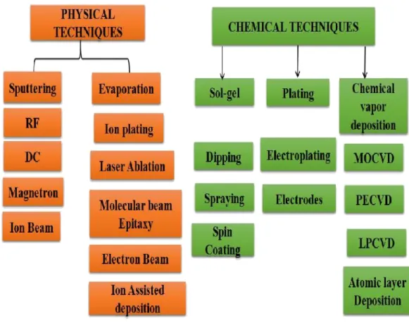
There is various innovation techniques available for making of thin films.These technologies can be divided into two main categories i.e.,chemical and physical techniques.The most exceptional techniques for mixture class are sol-gel, plating, compound vapor declaration (CVD), and atomic layer articulation (ALD).These techniques have been requested and presented in Figure.1.2.
Figure 1.2 Thin film deposition techniques.
1.2.1 Plating
Plating is a method of thin film deposition in which the surface of an object which is metals covered with a thin layer of another metal such as platinum, gold, and silver, etc.It is one of the most prehistoric thin film deposition technique, and in old ages, it has been used to deposit gold and other metals on various structures such as statues.This technique is still widely used for applications like corrosion protection, surface hardening, improve wearability, friction reduction, conductivity adjustment and radiation shielding etc.The technique has been classified into two main methods, i.e.,electroplating and electroless plating.In electroplating, a non-ionic coating is fabricated on a substrate by supplying electrons to an ionic metal.Generally, the equipment
that is being plated and a cathode where a film is being deposited.The electroless plating does not need external electrical power and takes place as a result of several simultaneous reactions in an aqueous solution.The reaction is executed when the reducing agent releases hydrogen and get oxidized, thus resulting in a negative charge on the surface of the part.
1.2.2 Sol-gel
Sol is defined as a stable dispersion of colloidal solid particles or polymers in a liquid where the particles are only suspended by Brownian motions.Whereas gel is stated which is formed when the solid and liquid are dispersed together and results in a porous, three continuous solid network which surrounds a continuous liquid phase.The sol-gel coating process takes place in following steps.
Ø Dispersion of colloidal particles in a liquid to fabricate a sol.
Ø Implementation of sol solution on different substrates through techniques such as spraying to fabricate the desired coatings.
Ø Polymerization of colloidal particles to get a continuous network state of gel by removal of stabilizing components.
Ø Development of coatings (amorphous/crystalline) by pyrolyzing the organic or inorganic components through heat treatment.
Some advantages of the sol-gel technique are; excellent adhesion, good corrosion protection, high purity products, low-temperature processing, and low cost of fabrication.The main sol-gel methods include dipping, spraying, and spin coating, etc.
1.2.3 Chemical Vapor Deposition
Chemical Vapor Deposition (CVD) is one of the most efficient and widely used method of materials processing.It is mostly used for thin film fabrication on a wide variety of substrates. The technique can also be implemented to develop bulk materials, composites, and different kinds of powders.The process typically involves a continuous supply of one or more precursors, i.e., chemical reactants to a substrate which is kept at a particular temperature and a thin film are deposited over the surface of the substrate as a result of chemical reactions.During this process, chemical by-products are also produced that are continuously removed out of the reactor along with unreacted precursors. It is an extremely flexible and diverse thin film deposition process.It can be used for deposition of films on a wide variety of substrates including glass, silicon wafers, flexible substrates and bulk objects.Similarly, it can be operated under a wide window of processing temperatures ranging from as low as 50° C to 1500° C.It is because of the supreme capability and efficiency of CVD technology that it has been continuously improved and evolved into a new trend.Some of the most notable trends are metal-organic chemical vapor deposition (MOCVD), plasma enhanced chemical vapor deposition, and low-pressure chemical vapor deposition (LPCVD).It is because of such advanced trends of CVD that its application circle has been greatly extended to new industries. The new trend of R2R-CVD has became a vital technique of electronic industry because its ability to fabricate mass production of the films at atmospheric condition.
1.2.4. Atomic Layer Deposition
Atomic layer deposition (ALD) is a subscale of chemical vapor deposition (CVD) capable of producing supreme quality thin films having low porosity, high density and excellent conformity
alternating, self-limiting surface reactions.This self-limiting reactions mechanism results in a saturated growth rate which means that the process reactions proceed to completion, and then stop. In this way, a precise amount of materials is deposited over the surface of the substrate regardless of the exposure to precursors once the saturation threshold is exceeded.
The mechanism of self- limiting growth provide ALD with unique advantages such as:
· Excellent conformity
· Good capability to produce sharp interfaces
· Precise thickness control
· High aspect ratio
· Processing of complex shapes and structures
ALD process involves a reaction sequence in which two independent surface reactions are separated in time.A substrate is placed in a chamber and is exposed to reactants and purge gases with the following sequence:
Ø Reactant A is pulsed into the reactor and reacts with the substrate Ø Products and unreacted reactant A are purged away
Ø Reactant B is pulsed into the reactor and reacts with the surface Ø Products and unreacted reactant B are purged away.
The new trend of ALD technique has been developed and introduced which encompasses the concept of atmospheric spatial ALD, and roll -to- roll processing.The result is an advanced, and efficient roll-to-roll atmospheric atomic layer deposition (R2R-AALD) system which is capable of rapid fabrication of thin films on flexible substrates ensuring mass production.[19]
1.3. Spatial Atomic Layer Deposition
Despite the fact that the conventional vacuum based ALD approach is very efficient in producing supreme quality films, there are limitations associated with it.The most notable of all is the time required to complete one ALD cycle.Scientific studies have reported that the cycle time may be as long as many minutes and result in deposition of films with a thickness of approximately one angstrom, which greatly reduces the efficiency of ALD technology.[19] Apart from that, the conventional ALD is a vacuum-based technology and has rarely been reported to be used for the fabrication of thin films under atmospheric pressure conditions.The size and design of the ALD reactor also affect the processing parameters of the ALD process. A complex and large ALD reactor would require a long purging time to be evacuated efficiently.Also, a very advanced and sophisticated valving system is needed to operate the ALD system in a steady state.This result in the complexity of the ALD system, and also the composition of the precursors is constantly varied in the reactor.Furthermore, the processable size of the stationary substrate in conventional ALD is very small due to which the ALD technology is unable to be used in applications requiring the cost-effective, large area and mass production of thin films.Such factors have become the source of motivation towards a more appropriate approach, i.e., spatial atomic layer deposition (SALD).[20,21] Unlike conventional vacuum based ALD where the precursors are separated in time, in spatial ALD (SALD) processes, the precursors are being separated in space.Figure.1.3 describes the conceptual design of SALD approach showing the continuous flow of precursors, inert gas, and film deposition over the movable substrate.
Figure1.3.Schematic of SALD reactor concept showing a continuous flow of precursors, inert gas, and film deposition over the movable substrate.[22]
1.4. Roll-to-Roll chemical &atomic layer Deposition Technique
Mass production of the thin film deposition is one of the key technologies for flexible electronics industries.R2R based ALD & CVD process is expected for continuous and mass production of various thin film fabrication shown in Figure.1.4.Sukang et al. reported roll to roll fabricated 30-inch of graphene films.[23] Recently Takatoshi et al. groups reported roll to roll MWP CVD deposited high-quality graphene thin films.[24] The roll-to-roll atomic layer deposition (R2R-ALD) is a special trend of spatial ALD. In R2R- ALD, the flexible substrate is continuously moving relative to the precursor sources and, therefore, the deposition rate is determined by the speed of the substrate rather than the cycle time of the precursor exposure sequence.[25] Since there is no requirement for pulsing and purging of precursors from a common volume, the growth rates of the deposited films are limited only by the surface kinetics and the reaction rates of each half cycle.Also, there is no need to clean the reactor walls because the precursors never interact with each other and thus avoid any deposition on the reactor walls. Such distinguished characteristics give a great edge and superiority to
R2R-ALD technology to process various kinds of flexible substrates such as polyethylene naphthalate (PEN), PET, and polyamide,etc.,on a large scale in a very low processing time, and this results in very high production at much lower costs.
Figure.1.4. The R2R deposition system: (a) R2R-SALD, (b) R2R-CVD.[24,25]
1.5. Inorganic transparent barrier coating on the polymers
The initial commercial transparent coating that appeared on the market was a silicon oxide SiOx
(deposited on polyethylene terephthalate (PET) films.Subsequently, HfO2, InSnO (ITO) ,
ZnSnOx, (ZTO) , SiOxNy, AlOXNycompounds have been tested for their barrier properties with
the polymer substrate.However, most wanted barrier materials in the market until now are aluminum silicon and Titanium oxide compounds due to its multifunctional properties.
1.5.1. Titanium dioxide (TiO
2
)
The unique and intriguing properties of nanostructured thin films have prompted tremendous motivation among researchers to explore the possibilities of using them in technological applications.In particular, the optical and electronic properties of nanostructured thin films have
been of very high interest due to their potential applications in the fabrication of microelectronics and optoelectronic devices.[26]The performance of the thin films for device applications is highly influenced by the crystallite size, morphology, phase and impurity type concentrations.[27] There is always an increasing demand for new technology for the fabrication of nanostructured thin films for functional devices in order to control the phase purity, morphology and the surface properties at the nanoscale which is of great interest to deliver distinctive properties.In this regard, many studies have been recently carried out to produce surfaces and films by tailoring nanostructure.Nanostructured thin films of titanium dioxide
(TiO2) have been regarded as subject of great deal of research due to its exceptional chemical,
electrical, optical properties and its potential applications diverse field such as (i) optoelectronic, (ii) photocatalytic (iii) solar cell (iv) photovoltaic, (v) self-cleaning coating (vi) antibacterial activity etc. Generally, TiO2nanostructured films exist in two phases viz. a) anatase and b) rutile.
Depending on the phase structure of TiO2, it can be employed for diverging applications.
Some well-known characteristics of TiO2are
• it is amphoteric in nature
• it is insoluble in water as well as acids
• it shows high room temperature resistivity, with a specific resistivity of 9500 Ω • it has a melting point of 1610º C and boiling point of 3000º C
1.5.2.Aluminium oxide (Al
2
O
3
)
Aluminum oxide is a combination of aluminum and oxygen with chemical formula Al2O3.The
most generally occurring of several aluminum oxides, and particularly identified as aluminum (III) oxide. It is generally called alumina. The oxides of aluminum materials have pontential applications refractories and abrasives due to their hardness , chemical inertness, high melting point non-volatility and resistance to oxidation and corrosion.[28-31]The significance of alumina as catalyst or catalytic support has likewise been widely applied for some chemical reactions.The trasnparency of alumina film and its variety of properties highly used the field of optics.[32]
Al2O3is an electrical insulator having high thermal conductivity.[33] Corundum or α-aluminum
oxide is the mostly occurring in crystalline form of aluminum oxide and its hardness make it appropriate for applications as a rough and as a component in cutting devices. conventional depsoition system requires higher enegy to produce Al2O3 thinfilm. But development of new cost-effective R2R-CVD &ALD techniques for fabrication of thin film with high purity and large area transparent films has attracted in many researchers.[24,34]
1.5.3. Silicon dioxide (SiO
2
)
Silicon dioxide, also called silica (from the Latin silex), is an oxide of silicon with the substance formula SiO2, most regularly found in nature as quartz and in different living organisms. In many parts of the world, silica is the significant constituent of sand.[35] SiO2 is the widely utilized
dielectric material in the semiconductor industry.The scientists have examined the qualities of SiO2
materials for different applications, for example, an insulator in capacitors for memory devices metal oxide semiconductor field effect transistors (MOSFETs), and a protection layer , a gas Diffusion barrier , flexible electronics , optoelectronics. SiO2has a large band gap (9.0 eV), a
low spillage present, great security from H2O, and low polluting influence levels in the film.
Consequently, SiO2is researched and generally utilized economically to alter numerous
applications over an expanded time duration. Transparent barrier coatings, such as silicon oxide (SiO2), on polymers, are receiving much attention in industries for pharmaceutical, food, and
beverage packaging applications. Conventional SiO2films are made by the thermal oxidation of
a silicon substrate under high temperatures. As novel electronic applications, for example, flexible and transparent devices have been rising quickly, deposition techniques have turned into a vital issue to accomplish smooth, conformal, powder free films, and low development
temperature. Conventional plasma enhanced chemical-vapor-deposition (PECVD) SiO2films
still indicate basic problems, for example, a nearly high development temperature, particle generation poor step coverage scope and a moderate growth rate. Accordingly, atomic layer deposition (ALD) has been recently inspired by an appropriate statement strategy for depositing conformal and uniform films under low-temperature deposition conditions.[34,20]
1.6. Scope of the Current Research
The conventional vacuum based CVD/ALD system have been capable to produce good quality thin films, but still they have some serious problems, such as low production, complexity operation and long processing time.Also the conventional CVD/ALD system only sitable for rigid device fabrications due to which it cannot be used for the application of flexible electronics. The current trend of new CVD/ALD technique has been introduced which the concept of atmospheric roll to roll CVD &ALD processing.The outcome is an efficient roll-to-roll atmospheric CVD & ALD system which is capable for rapid fabrication of thin films on flexible substrates ensuring large scale manufacturing.
Different thin films and various thin film architectures deposited by the R2R-ACVD & ALD process are to be investigate.Thin film materials of interest are Al2O3 SiO2, TiO2 and organic polymers the purposes for choosing these specific materials which has already been discussed in section 1.5.multilayer structures and other potential nanostructured engineering arrangements will likewise be examined.The benifits of Single and multilayer barrier architectures will be studied .
This work requires the use of the thin film characterisation techniques such as Field Emission Scanning Electron microscopy (SEM), vitality dispersive UV-Visible spectroscopy (UV) 3D surface profiler, Focused Ion Beam (FIB), Thickness measurement system, X-ray Photoelectron Spectroscopy (XPS), Contact angle measurement, Mechanical stability test, barrier permeation test.
CHAPTER 2
2. Experimental procedure
2.1. Materials and method
Tris(tert-pentoxy)silanol (TPS) was purchased from Sigma Aldrich for SiO2 source, and the
Trimethylaluminum (TMA) catalyst precursor was purchased from UP Chemical. Titanium
isopropoxide and water were purchased from UP Chemical for TiO2 source Polyvinylidene
difluoride (PVDF) pellets, dimethylformamide (DMF) and ammonia were purchased from Sigma Aldrich.
2.2. Roll-to-Roll Atmospheric chemical vapor Deposition of TiO
2
The experimental setup of R2R-ACVD for the deposition of TiO2 thin films is shown in
Figure.2.1.The CVD head for delivering the gas is installed over the movable PET substrate.A micro screw gauge used to adjust the head on vertically.The space between the head and the substrate was fixed at 300 μm.The CVD head has all the channels connected to it including
precursors, inert gas, and the exhaust. Nitrogen gas (N2) was used as a carrier gas and protected
the wall of the head.Two separate nitrogen cylinders were used to achieve the stable flow rates.
The temperature of the precursors, TTIP and water (H2O), was kept at 50º C, and the
temperature was maintained constant.In order to prevent the recondensation of the precursors, the temperature of gas delivery channels was maintained at 100ºC.The TTIP and H2O precursors
were injected into the CVD head through N2 gas at the flow rate of 500 SCCM and800 SCCM,
respectively, where the flow rate was controlled using a mass flow controller (MFC).The flow rate of separation nitrogen gas was kept higher (1000 SCCM) to effectively prevent the intermixing of the precursor in the reaction zone.The rotary pump was used for purging the waste gases, and the pressure beneath the CVD head was monitored by a vacuum gauge.The pumping speed of rotary pump was adjusted using the needle valves on the exhaust line.
Figure.2.1. Schematic diagram of the roll to roll atmospheric chemical vapor deposition.
A working pressure of 740 Torr, which is close to the atmospheric pressure of 760 Torr, was achieved by maintaining the pumping speed of 7 L /min. The web velocity of the PET substrate was varied in the range of 1–30 mm /S, and its tension was maintained at 10 KgF.A hot plate
was used to achieve and maintain the desired substrate temperature.The deposition of a TiO2thin
film on polyethylene terephthalate substrates with the average arithmetic roughness (Ra) of 1.45 nm was performed at low temperature in the range of room temperature to 75 and 100º C.
The precursor decomposition of (TTIP) is strongly related to the substrate temperature.The substrate temperature can lead to decomposition of the TTIP so that the room temperature and 50 °C temperature synthesized film shows high roughness and non-uniform in nature.This may be because of the slow decomposition occurred in this mechanism at atmospheric pressure
conditions. Further increasing the temperature to 75 and 100° C showed smooth and uniform morphology which proves that uniform film formation was occurred at high temperature (70° C) and further validates that precursor decomposition is temperature dependent and morphology were confirmed shown in Figure.2.2.The RMS roughness value of thin film at the room temperature, 50, 75 and 100 °C are 3.13, 2.76, 1.99 and 1.87 nm, respectively and it clearly indicates that temperature has a strong influence on the film morphology.
Figure.2.2. FESEM images of TiO2thin film on PET substrate. (a)Room temperature slow
decomposition nonuniform TiO2thin film, (b) Uniform TiO2thin film deposited at 100º C.
2.3. Al
2
O
3
deposited On PET substrate through R2R-AALD
The gas-delivery head had been installed over the movable substrate.The selected reactor head consist of multiple slits gas delivery channels.It is simple in design, compact, and can be easily installed in any R2R-ALD system.There are three inlets and one outlet at the top of the
connected to the inert gas channel.The outlet is connected to the exhaust channel for the sake of effective purging. A series of 25 slits has been fabricated in the head, three for each
precursor, seven for the inert gas, and twelve for the exhaust (purging).The exhaust slits, with the dimensions of 3mm × 90 mm, were chamfered at a specific angle (53.13°) to provide a chimney-shaped design which efficiently removes the by-products and unreacted gases from the surface of the substrate. The dimensions of the precursor slits and the inert gas slits are 1 mm × 90 mm.The precursor slits are separated from each other by the inert gas and exhaust slits, which effectively prevents them from intermixing.The ALD head has been designed in such a way that 5 ALD cycles are achieved when the substrate under go one complete pass i.e. the substrate is first translated forward and then translated backward. It means that one
complete pass is comprised of one complete forward and backward translation of the substrate
under the ALD head which results in 5 ALD cycles.Al₂O₃ ALD films have been deposited on
PET substrate using TMA and water at temperature of 50° C.The TMA and H2O precursors
were kept at a constant 30° C, and the gas delivery channels at 100° C, to prevent the recondensation of the precursors. The flow rates of the gases through the channels were
effectively controlled through mass flow controllers (MFCs).The TMA and H2O precursors
were delivered to the ALD head via N2gas at 500 sccm and 800 sccm, respectively.The flow
rate of the N2 separator gas was maintained at 1000 sccm in order to effectively prevent the intermixing of the two precursors in the reaction zone.A rotary pump was used for purging of the waste gases.A vacuum gauge was used to monitor pressure beneath the ALD head.The
experimental setup of R2R-AALD for the deposition of Al2O3thin films is shown in Figure.2.
Figure.2.3. Schematic diagram of the roll to roll atmospheric atomic layer deposition.
Table.2.1. The operational parameters of R2R-AALD system
Distance between head and substrate < 1mm
Web tension 1- 10 kgf
Web velocity 1- 10mm/sec
Substrate temperature RT - 100° C
Pressure 760 - 650 Torr
Exhaust rate 1-15 L/min
Precursors canisters temperature RT - 100° C
Precursors channels temperature RT - 100° C
2.4. R2R-AALD SiO
2
thin film On PET substrate
The SiO2 thin film deposition was done through the R2R-AALD system.The ALD head was
placed above the PET substrate, and the distance between the substrate and the head was ~ 400 μm.The precursor channel outlets and exhaust channels were connected to the head.The role of the nitrogen gas was to act as a carrier gas and inert separation gas.The major precursor is
Tri(tert-pentoxy) silanol (TPS) as SiO2 source, and trimethyl-aluminum (TMA) acted as a
catalyst.[36] The canister of TPS maintained at 110° C, and the TMA was maintained 10oC.The
precursor's channels were maintained at 100o C for preventing the recondensation of the
precursor.The delivered flow rate of the precursor TPS and catalyst TMA were fixed at 100 SCCM and 50 SCCM respectively.To prevent the inter mixing of the precursors, nitrogen gas flow rate was fixed at 1000 SCCM. The flow rates were adjusted by the mass flow controllers (MFC).The unreacted gas purged out through the rotary pump, and the reaction pressure was maintained at 740 Torr.This reaction pressure was closely related to the atmospheric pressure.
The web velocity of the PET substrate was fixed at 7 mm s-1and the tension was fixed at 10 KgF.
This sio2 thin film was fabricated at 90o C on a flexible PET substrate. The Photographic illustration of the roll to roll atmospheric atomic layer showed in Figure.2.4.
Figure.2.4. The Photographic illustration of the roll to roll atmospheric atomic layer deposition and with their component's information.
2.5. PVDF deposition through EHDA technique
EHDA technique can be used to deposit a variety of materials with supreme and uniform thin films.[37-41]The required flow rate was maintained by the syringe pump (Harvard Apparatus, PHD 2000 Infusion). The PVDF ink filled syringe was connected with the metallic capillary with a diameter of 210 μm.The high electric field between metallic capillary and ground was applied. The EHDA operation had several modes of deposition such as dripping, micro-dripping, stable, unstable, and multi-jet process whose pictures were captured through the high-speed CCD
camera.The substrate stage was capable of moving in the X-Z direction, and the metallic holder could move in the Y direction.After the careful adjustment between the nozzle and substrate, the uniform spray result was achieved.The PVDF organic thin film achieved at room temperature along the substrate speed of 0.35 mm/sec.The uniform deposition was achieved at the flow rate of 400 μl/h. The prepared sample was sintered at 90° C for 3 hours.The EHDA deposition was performed under various flow rates at a fixed distance of 20 mm. The electrical current was increased for every flow rate by the applied voltage between the stage and nozzle. Optical image representation of the electrohydrodynamic atomization system showed in Figure.2.5.
Figure.2.5. Optical image representation of the electrohydrodynamic atomization system for thin film deposition experiment.
2.6. Multilayer thin film preparation
The hybrid PVDF/SiO2 multilayer barrier thin film was fabricated by using combined
R2R-AALD and EHDA deposition techniques.The schematic diagram of the hybrid barrier thin film
preparation is presented in Figure.2.5.The first layer of inorganic SiO2 thin film was deposited
by R2R-AALD. The growth rate of the SiO2 thin film in a single pass was maintained at ~ 0.90
nm/pass.The second layer of the organic material PVDF was deposited through EHDA deposition process. After depositing the organic thin film, it was sintered at 70° C for 4 hours.
Figure.2.6. Schematic illustration of the multilayer barrier film preparation as well as thickness of each film
2.7. Thin Film Characterizations
The fabricated thin films were successfully characterized through various techniques. 1. The thickness of the films was measured using a state of the art, nondestructive, thin
film thickness measurement system K-MAC ST4000-DLX, and Focused Ion Beam 2. The morphology and conformity of the films were observed using a JSM-6700F
FESEM and NanoView high accuracy 3D nano non-contact surface profiler.
3. The chemical composition level was analyzed using VG Microtech XPS analysis equipment using Mg Ka radiation from an X-ray source operating at 12 kV, 15 mA. The XPS analysis was also conducted using another model, i.e., PHI Quantera II VG X-ray photoelectron spectroscopy (XPS) equipment.
4. The contact angle measurements were carried out using SEOPhoenix 3000 Touch using deionized water.
5. The UV characterization was performed using a Shimadzu UV-3150 UV/VIS/NIR spectrophotometer.
6. The electrical characterization was done by using Agilent B1500A Semiconductor Device Analyzer coupled with an MST8000C Probe Station was used.
CHAPTER 3
3. Result and discussion
3.1. Low temperature deposited TiO
2
Thin Films
Titanium dioxide (TiO2) is an inexpensive photoactive material, lightweight and eco-friendly in
nature. It is a commercial material that has been primarily used as a pigment for coating application due to its highly visible light scattering nature.[42] It has a high refractive index
and is chemically stable in the UV and visible region.[43] TiO2has been widely used for various
applications such as dielectric materials,[44] antireflection coatings, self-cleaning surfaces,[45,46] dye-sensitized solar cells,[47] and a photocatalyst[48,49], TiO2 has the four phases, anatase (tetragonal), rutile (tetragonal), brookite (orthorhombic), and an amorphous phase.[50] TiO2 thin films have been fabricated by various methods such as sol-gel, spray pyrolysis, electron beam evaporation, sputtering, plasma-enhanced chemical vapor deposition, metal– organic chemical vapor deposition, and atomic layer deposition.[51] Chemical vapor deposition (CVD) is the most commonly used method in the field of material processing technology, and by using this technique, the solid material is deposited as a film on the substrate material with a uniform distribution over a large area. A variety of materials can be deposited as a thin film by CVD with low defect density and high purity. CVD can be utilized for the production of MEMS technology[52] and graphene fabrication.[53] Different types of CVD techniques for fabricating thin films include plasma-enhanced chemical vapor deposition (PECVD), metal–organic chemical vapor deposition (MOCVD), atmospheric pressure chemical vapor deposition (APCVD), and plasma-assisted chemical vapor deposition (PACVD). Advantages of APCVD are that the film could be synthesized using low-cost equipment and the temperature and gas flow can be controlled to obtain a uniform film over a large surface area.
Compared to other techniques, this method could be used to fabricate the film without vacuum conditions.[54] The roll-to-roll CVD technique is a well-known method for the mass production of the films that is cost-effective, and it is highly useful for industrial applications.
Many researchers have deposited TiO2 films at high temperatures, but only a few were able to
achieve a low-temperature deposition of TiO2.Maruyama et al. fabricated amorphous TiO2 film
by applying atmospheric pressure CVD on glass and silicon substrates with temperatures ranging
from 200 to 500ºC.[55] Masuda deposited an amorphous TiO2 thin film on the silicon substrate
at room temperature.[56] Sun et al. synthesized amorphous TiO2film on glass and PET substrate
at room temperature.[57] Yamauchi et al. deposited TiO2 thin film on the quartz substrate by
PECVD with temperatures in the range of 300– 400ºC.[58] Lee et al. deposited a TiO2thin film
on a silicon substrate by PECVD for the substrate temperature in the range of 100–400ºC.[59]
Mathur deposited TiO2 thin film by DC plasma-assisted CVD below 200ºC.[60] Kolouch
deposited TiO2thin film on the glass and silicon substrate by using PECVD with temperatures as
low as 120º C.[61] Previously Sun et al.[62] synthesized a thin film of TiO2at room temperature
on a movable substrate. The roll-to-roll atmospheric chemical vapor deposition (R2R-ACVD) system is the best technique to fabricate thin film on a polymer substrate, and it plays a vital role in flexible electronics and has tremendous applications because of its light weight and
mechanical stability. In the present study, R2R-ACVD TiO2 thin film was deposited on a
movable PET substrate with different substrate temperatures including room temperature, 50, 75,
and 100ºC. The structure and morphology of the TiO2films have been characterized by the field
emission scanning electron microscopy and 2D surface profiler. Electrical, optical, and chemical properties were determined through current-voltage (I–V) measurement, UV–visible spectrum, and X-ray photoelectron spectroscopy, respectively.
3.1.1. Film growth
The deposition rate of TiO2 films over the PET substrate under different temperatures was determined.The observed deposition rate corroborated that temperature has a significant influence on the film formation.The nature of precursor and its stability played a vital role in the deposition rate and topography of the as-deposited film. In the present study, TTIP was used as a
precursor due to the very fast hydrolysis rate and the easy formation of TiO2which may increase
with an increase in the temperature.
Figure .3.1.The deposition rate (nm/min) of the TiO2thin film increased while increasing the temperatures such as RT, 50, 75 and 100 °C.
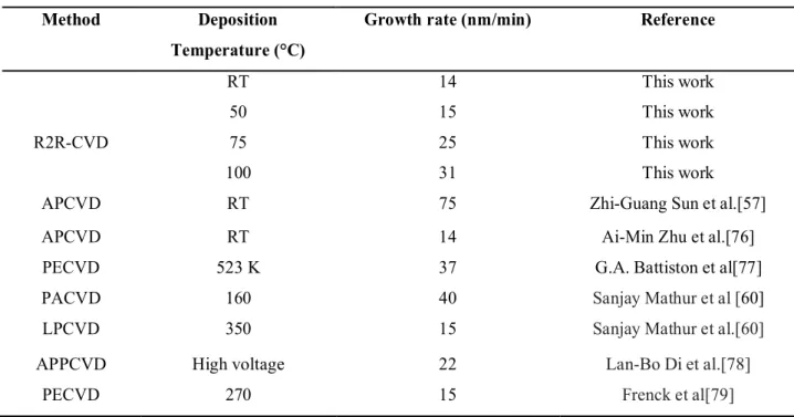
The 25- cm-long sample was moved back and forth repeatedly for 9.3 min, being continuously exposed to the precursor for the whole duration of the process. The deposition rate of the observed film thickness was 14, 15, 25, and 31 nm per minute with room temperature, 50, 75, and 100º C, respectively. This clearly indicates that the temperature depended on the film
deposition rate as shown in Figure.3.1.The total thickness of the film at room temperature, 50, 75,
and 100ºC was 131, 144, 239, and 310 nm, respectively. The TiO2 thin film prepared at 100ºC
possesses a larger thickness than the lower substrate- temperature film (RT—75ºC). This result indicates that film deposition rate might be dependent on the substrate temperature.[63] Film thickness attained by the R2R-ACVD method is compared with the previously reported literature (Table.3.1). The results revealed that the obtained film thickness is quite comparable to the other reported methods; however, in this method, low temperature and pressure were used for deposition.
Table 3. 1: Summary of the growth rate observed in the Previous Reports
Method Deposition Growth rate (nm/min) Reference
Temperature (°C)
RT 14 This work
50 15 This work
R2R-CVD 75 25 This work
100 31 This work
APCVD RT 75 Zhi-Guang Sun et al.[57]
APCVD RT 14 Ai-Min Zhu et al.[76]
PECVD 523 K 37 G.A. Battiston et al[77]
PACVD 160 40 Sanjay Mathur et al [60]
LPCVD 350 15 Sanjay Mathur et al.[60]
APPCVD High voltage 22 Lan-Bo Di et al.[78]
3.1.2. Surface morphology
FE-SEM images of the TiO2 thin film deposited at different temperatures are shown in
Figure.3.2.The FE-SEM image of the as-deposited TiO2 thin film at room temperature and at 50ºC showed that the surface of the film has highly rough morphology (Figure.3.2 (a) and (b)). These FE-SEM results match closely with the results reported in the literature.[64] By further increasing the substrate temperature, the surface roughness of the film diminished (Figure.3.2 (c) and 3(d)). This observation validated the fact that the smooth film surface can be obtained at high substrate temperature, and these results were well matched with what was reported in the literature.[65]The observed nonuniform deposition at room temperature may be due to the slowly occurring diffusion, and it may be due to the slow decomposition of precursor material (alkoxide).The growth of the film formation takes place via diffusion followed by nucleation mechanism.At low temperatures, slow diffusion occurs and may be due to the slow decomposition of the precursor material [66] which results in the uneven nucleation sites for film growth. However, in the case of high temperatures, the decomposition of the precursor is enhanced by the substrate temperature, which results in the more nucleolus formation in the substrate.This enables the uniform diffusion of precursor molecule on the bulk surface. The observed FE-SEM images validated the aforementioned results.
Figure.3.2. FESEM images of TiO2 thin film on PET substrate. Nonuniform TiO2 thin film deposited at (a) RT, (b) 50 °C and uniform TiO2thin film deposited at (c) 75 °C, (d) 100 °C.
Moreover, to further support the dependence of surface morphology on the substrate temperature,
the prepared TiO2 films were characterized by a 2D nanosurface profiler.Figure.3.3 shows that
the room-temperature-deposited TiO2 film revealed high surface roughness as compared to
others. When the temperature increases, the surface roughness of the film decreases.
[67] The temperature-dependent surface roughness results were matched with the reported
results.The 2D surface profile of the TiO2 films grown at room temperature (RT), 50, 75, and
100ºC is shown in Figure.3.3.These 2D surface profile results corroborate with the FE-SEM and film deposition rate measurement results.The root means square (RMS) value extracted from the 2D nanosurface profiler results showed a decreasing value with increasing substrate deposition temperature.
Figure.3.3. 2D surface profile, images of the TiO2thin film on PET substrate. High
roughness obtained the TiO2thin film deposited at (a) RT, (b) 50 °C and low roughness obtained the TiO2thin film at (c) 75 °C and (d) 100 °C.
The RMS value for room temperature, 50, 75, and 100ºC is 3.13, 2.76, 1.99, and 1.87 nm, respectively, clearly indicating that temperature has a significant influence on the surface of the
film. The least value of Rq 1.87 nm and Ra value 1.55 nm is observed for TiO2film deposited at
100ºC. The observed least RMS for TiO2 prepared at 100ºC is better than the earlier reported
methods.[68,69] The topography of the film decides its optical and other properties. Thus, the
3.1.3. Optical transmittance
UV–Vis spectrum of TiO2 thin films prepared by the R2R-ACVD method at the different
temperatures is shown in Figure.3.4.The results revealed that 91.2% transmittance was observed
for TiO2thin film prepared at 100ºC and it is quite higher than the low substrate temperature (RT,
75ºC).All the prepared TiO2 thin films showed transmittance from 86% to 91.2% in the visible
range (400–800 nm). Hocine et al.[70] and other research groups reported that 80–90.2%
transmittance was observed for TiO2 thin films prepared by different CVD methods under
different temperatures.In comparison with the earlier reported results, the observed 91.2% transmittance of this study and high surface smoothness at low substrate temperatures are the new reasons for adapting the R2R-ACVD film coating method.Furthermore, the different optical transmittance results further support the morphology-based optical property of the prepared film. FE-SEM and surface profiler clearly show that the room temperature film has a high roughness which leads to low transmittance (86%).From these results, we conclude that it can be a promising candidate for optoelectronics application.[71]
Figure 3.4. Optical property of TiO2thin film on the PET substrate by R2R-ACVD at room
temperature to 100 °C. The optical transmittance was observed at 91 % in the visible region for 100 °C.
3.1.4. Compositional analysis
The X-ray photoelectron spectroscopy (XPS) analysis was performed to understand the oxidation
state and the defects present in the prepared TiO2 films.The high-resolution XPS spectra of Ti2p
and O1s of TiO2film prepared at different substrate temperatures are shown in Figure 3.5(a) and
(b).From the O1s spectra, it is observed that there are no significant changes in the peak intensity with an increase in the coating temperature; however, the small shift in the peak position
indicates the presence of defects in the prepared TiO2 film.The changes in the binding energy of
O1s state clearly show that O concentration on the TiO2 film was increased.The atomic
percentage result also indicates that oxygen concentration was increased with an increase in the temperature (Table.3.2). Moreover, carbon (%) content declined with an increase in the substrate
temperature, indicating that more decomposition of the precursor occurred. Similarly, the higher percentage of Ti was observed with an increase in the temperature, indicating the denser Ti concentration.The observed atomic concentration of Ti, O, and C evidently supported that film thickness increased by increasing the temperature.Moreover, the high-resolution XPS spectrum of Ti2p displays two peaks at 458.7 and 463.4 eV that are attributed to the Ti 2p3/2 and Ti 2p1/2
levels of TiO2 and validates the successful synthesis of TiO2 film, and the valence of Ti is four
(Figure.6b).However, when increasing the temperature from RT to 100ºC, the binding energy is shifting from 457.4 eV to 458.7 eV respectively.This may be because when the temperature increases titanium oxides lost oxygen which leads to the existence of Ti4+ and Ti3+ in the
synthesized film.[72] However, the synthesized TiO2film is highly stable which is in accordance
with the FE-SEM and UV–Vis spectroscopy analysis results.[73]
Table 3.2: Atomic Composition of TiO2 film prepared by R2R-ACVD with different
substrate temperature
TiO2 RT 50 °C 75 °C 100 °C
O1s 61.9 O1s 64.8 O1s 63.1 O1s 65.0
Atomic % Ti2p 27.8 Ti2p 29.5 Ti2p 28.5 Ti2p 29.1
Figure.3.5. The XPS spectra of R2R-ACVD TiO2films deposited at different temperatures (a) O 1s and (b) Ti 2p from TiO2films
3.1.5. Electrical properties
Electrical properties of the TiO2 films were analyzed using the Agilent B1500A Semiconductor
Device Analyzer coupled with a MST8000C Probe Station. Current (I) voltage (V) characteristics of the TiO2 thin film fabricated at different temperatures were measured. Initially, the metallic contacts were made on the top of the film using Ag ink by drop casting method. Subsequently, the measurements were carried out under room temperature with the help of two probes on the circular-shaped Ag metallic contacts of the films. Measurement of the metallic contacts distance is 4 mm. Figure.3.6. shows I–V behavior of the R2RACVD method-deposited TiO2 film indicating a good insulating nature. Moreover, the TiO2 film prepared at 100º C
showed 1.18 nA current, and other TiO2 films showed an extremely low current (pA). TiO2 thin
films deposited at room temperature are smaller in thickness than the film deposited at 50, 75, and 100ºC. Also, films deposited at room temperature showed extremely lower current (pA)
because of their discontinuity and nonuniformity. These low-current TiO2films could be used in the field of biosensor development and as a good insulator for electronics applications. [74,75].
Figure.3.6.The I-V characteristics of TiO2film at RT to 100 °C temperature grown on PET substrate
3.2. Single layer Al
2
O
3
deposited on PETsubastrate
The trimethylaluminum [Al (CH₃)₃, TMA] and water (H₂O) is a important precursor for
Al₂O₃ thin film. Al₂O₃ can be coated on polymer substrate due to Al₂O₃ can be deposited at
low temperature.[80] The Al₂O₃ coat on polymers provide a pathway to fabricate
inorganic-organic composites with novel properties.ALD coated Al₂O₃ thin films can be utilized to gas
barrier on polymeric substrates to prevent H₂O and O₂ permeation.Also Al2O3has potential
use in microelectronics and microelectronics devices. Many researcher have examined and
lower many have broke down it under lower temperature.[80-82] The low temperature ALD process is difficult also it need careful assessment for processing.
Previously, different model of roll-to- roll based ALD system have been reporeted to fabricate
thin films on various substrate.[83,84] Dickey et al. have shown the deposition of Al2O3 and
TiO2barrier thin films at 75 ºC on polymeric substrates through the vacuum based roll to roll
ALD. This system ability to produce barrier thin films at 12 nm on a 10 cm PET web with water vapor transmission rates in the scope of 10-4 g/m2/day under the web velocities of 1
m/s.[85] Kamran et al. achievd a WVTR of ~10−3 g/m2/day under the web speed of 7 mm/s
for Al2O3thin film with thickness range from 15-40 nm.[86] Groner et al. fabricated very thin
(10-25 nm) Al2O3film and achieving WVTR of 1× 10⁻³g m−2day.[87] They have suggested
that the Al2O3deposition can be possible through low substarte temperature.
In this research work R2R-AALD has been described for and its application has been
discussed about for the development of low temperature Al2O3 films for single layer barrier
applications. The precursors TMA and water that were kept at a steady temperature of 30º C. The gas delivery channels were kept at 100 °C to prevent the recondensation of the precursors.
The precursors. (TMA and H₂O) were supplied to the ALD head with the help of N2gas at the
flow rates of 700 SCCM and 1000 SCCM respectively and the flow rates through the channels were controlled by the mass flow controllers (MFCs).The individual seperator nitrogen gas was kept at (1200 SCCM) to avoid the intermixing of precursors in the reaction region. The rotary pump was using to remove unreactant gas from the reaction chamber and ALD was continuosly monitored by vaccum gauge. The nearly atmospheric pressure of 750 Torr was achieved by keeping up the pumping speed of 7 L/minute.The web speed of the PET substrate was changed in the range of 1 mm/sto 10 mm/s and its tension was kept constant at
10 kgF. The required substrate temperature was achieved through a hot plate. The Al₂O₃ thin film deposition was done at a low temperature range of room temperature (RT) to 50 ºC on PET substrates.
3.2.1. Film Growth
The growth rate per cycle is important characteristic of ALD system.It gives fundamental information about the effectiveness, reliability and the nature of ALD process. In our
investigation, the growth rates of Al₂O₃ thin films done by R2R-AALD and measuring the
film thicknes by thickness as number of ALD cycles.Figure.3.7(a) indicates thickness of the
Al2O3 films as a working process cycles deposited at 50 °C under velocity of 7 mm/s.The
design of the ALD head achived 5ALD cycles in a one complete pass i.e.forward and backward direction.The exposure times of the precursors based on the speed of the moving web. In this manner, the optimized self-limiting ALD process was affirmed at 50 °C by measuring the film thickness against the web speeds.The Figure.3.7.(b) shows high uncontrolled development rates are recorded for the films deposited under the web speed of more than 7 mm/s.
Figure.3.7.Thickness Al2O3films on PET substrates versus the number of process cycles at 50 °C under the web velocity of 7mm/second (a), and growth rates of the Al2O3films
versus the web velocity (b).
3.2.2. Surface Morphology
The surface morphology of the Al2O3 films deposited at 50 °C by R2R-AALD on PET
substrates was examined through FESEM and nano surface profiler.Figure 3.8 (a), (b), shows the
FESEM images of the bare PET substrate, and 50 °C deposited Al2O3on PET, respectively. The
results clearly showed uniform and smooth Al2O3 thin films have been deposited on PET
substrates through R2R-AALD.The surface morphology was additionally studied with 3D nano
surface profiler. The 2D surface profile results of the 50 °C grown Al2O3films grown shown in
Figure. 3.8.(c). 2D surface profile results shows very low roughnes (Ra) values of 1.57 nm have been recorded for the Al2O3thin films under at 50° C.
Figure 3.8. FESEM images of the bare PET substrate (a), Al2O3-coated
PET at 50 °C (b), and 2D surface profile of the Al2O3films grown at 50 °C
(c).
3.2.3.Compositional Analysis
The Al₂O₃ thin films deposited at 50° C through R2R-AALD were subjected to X-ray
photoelectron spectroscopy analysis to confirm chemical composition level of the thin