* Dept. of Energy IT Engineering, Far East University
★ Corresponding author
E-mail:[email protected], [email protected], Tel:+82-43-880-3292
※ Acknowledgment
This work was supported by the Korea Institute of Energy Technology Evaluation and Planning(KETEP) and the Ministry of Trade, Industry & Energy(MOTIE) of the Republic of Korea (No. 20194010201810, No. 20194010000050).
This research was supported by the MOTIE (Ministry of Trade, Industry, and Energy) in Korea, under the Fostering Global Talents for Innovative Growth Program (P0017308) supervised by the Korea Institute for Advancement of Technology (KIAT)
Manuscript received May. 17, 2021; revised Jun. 12, 2021; accepted Jun. 25, 2021.
This is an Open-Access article distributed under the terms of the Creative Commons Attribution Non-Commercial License (http://creativecommons.org/licenses/by-nc/3.0) which permits unrestricted non-commercial use, distribution, and reproduction in any medium, provided the original work is properly cited.
1,200V 급 Trench Gate Field stop IGBT 공정변수에 따른 스위칭 특성 연구
A Study on Switching Characteristics of 1,200V Trench Gate Field stop IGBT Process Variables
조 창 현
*
, 김 대 희*
, 안 병 섭*
, 강 이 구* ★
Chang Hyeon Jo
*
, Dea Hee Kim*
, Byoung Sup Ahn*
, Ey Goo Kang* ★
Abstract
IGBT is a power semiconductor device that contains both MOSFET and BJT structures, and it has fast switching speed of MOSFET, high breakdown voltage and high current of BJT characteristics. IGBT is a device that targets the requirements of an ideal power semiconductor device with high breakdown voltage, low V
CE-SAT, fast switching speed and high reliability. In this paper, we analyzed Gate oxide thickness, Trench Gate Width, and P+Emitter width, which are the top process parameters of 1,200V Trench Gate Field Stop IGBT, and suggested the optimized top process parameters.
Using the Synopsys T-CAD Simulator, we designed IGBT devices with electrical characteristics that has breakdown voltage of 1,470 V, V
CE-SAT2.17 V, Eon 0.361 mJ and Eoff 1.152 mJ.
요 약
IGBT는 MOSFET과 BJT의 구조를 동시에 포함하고 있는 전력반도체 소자이며, MOSFET의 빠른 스위칭 속도와 BJT의 고 내압, 높은 전류내량 특성을 갖고 있다. GBT는 높은 항복전압, 낮은 V
CE-SAT, 빠른 스위칭 속도, 고 신뢰성의 이상적인 파 워 반도체 소자의 요구사항을 목표로 하는 소자이다. 본 논문에서는 1,200V 급 Trench Gate Field Stop IGBT의 상단 공정 파라미터인 Gate oxide thickness, Trench Gate Width, P+ Emitter width를 변화시키면서 변화하는 Eoff, V
CE-SAT을 분석하 였고, 이에 따른 최적의 상단 공정 파라미터를 제시하였다. Synopsys T-CAD Simulator를 통해 항복전압 1,470V와 V
CE-SAT2.17V, Eon 0.361mJ, Eoff 1.152mJ의 전기적 특성을 갖는 IGBT 소자를 구현하였다.
Key words : IGBT, V
CE-SAT, Switching loss, Gate oxide, Cell Pitch, Trench Gate
117
Ⅰ. 서론
IGBT(Insulated Gate Bipolar Transistor)는 MOSFET (Metal Oxide Semiconductor Field Effect Transistor) 과 BJT(Bipolar Junction Transistor) 구조를 동시 에 포함하고 있으며, MOSFET의 빠른 스위칭 속 도와 BJT의 고 내압, 높은 전류내량의 장점을 결 합한 특성을 갖고 있다. IGBT는 고 전압을 제어하 는 소자로 고 신뢰성과 고효율을 필요로 하며 신재 생 에너지 발전기, 전기자동차, 전원 공급 장치, 변 환기, 모터제어 등의 분야에서 효율 향상을 위해 사용되고 있다. 특히 신재생 에너지 및 전기자동차 시장규모가 확대됨에 따라서 전력반도체의 응용범 위가 확대되고 있는 상황이다[1]-[6].
IGBT는 구조의 차이에 따라, Punch Through, Non-Punch Through, Field Stop IGBT로 분류된 다[2], [5]. 그 중 Field Stop IGBT는 Back 공정을 통해 Buffer(Field Stop Layer)층을 형성하여 높은 항복전압을 갖고, 짧은 Current Tail을 가지 장점이 있다[1], [5].
IGBT는 one-type Carrier인 MOSFET과 달리 two-type Carrier소자이기 때문에 높은 전류량을 갖는 것이 특징이다[1]. 하지만 이런 IGBT의 two- type Carrier로 인해 MOSFET보다는 느린 속도를 갖고, Drift층에 소수 캐리어 축적으로 인한 Turn- off 시 tail current 현상이 생기는 것이 단점이다.
이러한 tail current를 완화시키기 위해 Field stop IGBT에서는 Field stop Layer의 농도와 크기를 변 화시키거나 Gate oxide 크기를 변화시키는 등 다양 한 방법이 제시되고 있다. 이러한 Field Stop Layer 농도와 크기 변화 및 Gate oxide 크기를 변화시키 게 되면 전도도 변조 현상 및 채널영역의 소수캐리 어 축적이 감소하여 온-상태 전압강하(VCE-SAT)가 증가하는 Trade-off관계를 가지게 된다[2], [5], [7].
본 논문에서 이러한 Trade-off 관계를 분석하고, IGBT Switching 특성 최적화를 위해서 IGBT 상 단 공정 파라미터인 Gate oxide thickness, Trench Gate Width, P+ Emitter width의 공정변수에 따라서 변화하는 Eoff, VCE-SAT을 Synopsys사의 Sentaurus TCAD를 사용하여 분석하였고, 이에 따른 최적 공 정파라미터를 제시하였다.
Ⅱ. FS-IGBT 구조와 스위칭 회로
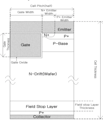
2.1 Field-stop IGBT의 구조Fig. 1. Structure of Trench Gate Field stop IGBT.
그림 1. Trench Gate Field stop IGBT의 구조
그림 1은 Trench Gate Field stop IGBT의 구조 를 나타내었고, IGBT를 설계하기 위해 기본적인 파라미터로 Cell Thickness는 120um, N-Drift의 비저항은 60Ω×cm을 고정하였다. 소자의 항복전압 은 마진율 20%를 고려하여 1,440V이상을 목표로 한다[3], [4], [6].
2.2 IGBT Switching simulation을 위한 회로와 파라미터
Fig. 2. Configure Circuit for Switching characteristics simulation.
그림 2. Switching 특성 simulation을 위한 Circuit 구성
Switching Simulation Conditions Unit Tvj=25°C, V
CC=600V, I
C=30.0A,
V
GE=0.0/15.0V, dv/dt=600V/0.1us R
G=10.0Ω, Lσ=70nH, Cσ=50pF
mJ
Table 1. Circuit parameters for switching characteristics simulation.
표 1. Switching 특성 simulation을 위한 회로의 파라미터
그림 2에서 IGBT의 Switching 특성 Simulation 을 위한 Circuit을 나타내었고, 표 1에 Simulation 조건을 나타내었다.
상온 25℃의 조건에서 Collector에 600V를 인가 하고, Gate와 Emitter 간 전압이 0V/15V 일 때 스 위칭 특성을 측정하였다.
Ⅲ. FS-IGBT 스위칭 특성 분석
3.1 Gate Oxide에 따른 전기적 특성 분석600 700 800 900 1000
0.3 0.6 0.9 1.2 1.5
1.8 Eon
Eoff
Gate Oxide (A)
E on ( m J)
0.95 1.00 1.05 1.10 1.15 1.20
E o ff (m J)
Fig. 3. Variation in Eon and Eoff according to Gate Oxide Thickness.
그림 3. Gate Oxide thickness에 따른 Eon과 Eoff의 변화
Gate Oxide(Å) Eon(mJ) Eoff(mJ) Eon+Eoff(mJ)
600 0.5392 1.0429 1.5021
700 0.5582 1.0068 1.485
800 0.5894 0.9967 1.5061
840 0.6143 0.9936 1.5279
880 0.6694 0.9915 1.5809
900 0.7467 0.9876 1.6543
930 1.2542 0.9705 2.1447
950 1.9825 0.8567 2.7592
Table 2. Variation in Eon and Eoff according to Gate Oxide Thickness.
표 2. Gate Oxide thickness에 따른 Eon과 Eoff 변화
Fig. 4. Switching characteristics when Gate Oxide Thickness is 600Å, 950Å.
그림 4. Gate Oxide Thickness가 600Å, 950Å일 때 Switching 특성
600 650 700 750 800 850 900
2.4 2.5 2.6 2.7 2.8 2.9 3.0
V C E -S A T ( V )
Gate Oxide ( ) Å VCE-SAT
Fig. 5. V
CE-SAT(V) characteristics when Gate Oxide Thickness is 600Å, 950Å.
그림 5. Gate Oxide Thickness가 600Å, 950Å일 때 V
CE-SAT(V) 특성
Gate Oxide Thickness(600∼950Å) 증가에 따른 Eon과 Eoff 특성을 비교하였으며 시뮬레이션 결과 는 그림 3에 나타내었다.
게이트 산화막 두께가 증가함에 따라 문턱전압이 증가하게 되어 VCE-SAT은 증가하고 Eoff는 감소하 는 특성을 보이고 있다. 게이트 산화막 크기가 900 Å 이상이 될 때 Eon이 급격하게 증가하게 되는데, 문턱전압의 증가로 Turn-on 초기구간에서 충분한 전류를 공급하지 못하여 Collector와 Emitter간 전 위차가 증가한 구간에 따라 Eon이 급격하게 증가 하는 것을 그림 4를 통해 확인할 수 있다.
Gate Oxide Thickness는 Eon 특성과 Eoff 특성 을 고려하여 700Å으로 고정하였다. Gate Oxide Thickness의 증가에 따라 VCE-SAT이 증가하는 경
향을 보였고, 스위칭 손실(Eon + Eoff)는 880Å이 하에서 1.58mJ 수준의 값을 나타내고 있으나, 900 Å 이상부터 스위칭 손실이 급격히 증가하는 경향 을 확인할 수 있다.
3.2 Gate width에 따른 전기적 특성 분석
0.4 0.5 0.6 0.7 0.8 0.9 1.0 1.1 1.2 1.3 2.0
2.1 2.2 2.3 2.4 2.5 2.6
Vce-sat Eoff
Trench Gate Width (um)
V ce -s at ( V )
1.15 1.20 1.25 1.30 1.35
E o ff (m J)
Fig. 6. Variation in V
CE-SATand Eoff according to Trench Gate Width.
그림 6. Trench Gate Width에 따른 V
CE-SAT과 Eoff의 변화
Half cell pitch를 2.0um으로 고정한 상태에서 Trench Gate width를 0.5um에서 1.2um까지 0.1um 씩 증가시키면서 Eoff와 VCE-SAT특성을 확인하였다.
Trench Gate width가 증가함에 따라 그림 6에 주어진 바와 같이 VCE-SAT이 감소하며 Eoff는 증가 하는 경향을 나타내고 있다. Trench Gate width가 증가함에 따라서 게이트 하단의 면적의 증가하게 된다. 게이트 하단 면적 증가에 따라 injection enhancement 효과가 증가되어 VCE-SAT은 감소하지 만, 주입된 hole carrier의 증가로 Turn-off 손실은 증가하는 경향을 보이고 있다.
3.3 P+ Emitter Width에 따른 전기적 특성 분석
0.2 0.3 0.4 0.5 0.6 0.7
2.10 2.15 2.20 2.25 2.30 2.35 2.40
V ce -s a t ( V )
P+ Emitter Width (um)
Gate Width (0.8) Gate Width (1.0) Gate Width (1.2)
Fig. 7. V
CE-SATaccording to P+ Emitter Width.
그림 7. P+ Emitter Width에 따른 V
CE-SAT특성
0.2 0.3 0.4 0.5 0.6 0.7
0.87 0.90 0.93 0.96
E of f ( m J)
P+ Emitter Width (um)
Gate Width (0.8) Gate Width (1.0) Gate Width (1.2)
Fig. 8. Eoff according to P+ Emitter Width.
그림 8. P+ Emitter Width에 따른 Eoff 특성
Trench width가 0.8, 1.0, 1.2(um) 일 때 P+ Emitter Width 변화에 따른 전기적 특성을 확인하였다.
Emitter 영역의 P+을 제외한 상단의 파라미터를 고정하였기 때문에 Cell pitch도 함께 변화한다.
그림 7, 8에 주어진 바와 같이 P+ Emitter Width 증가에 따라서 VCE-SAT은 감소하고 Eoff 는 증가하 는 경향을 나타내고 있다.
3.4 최종 설계한 FS-IGBT의 전기적 특성
0 200 400 600 800 1,000 1,200 1,400 1,600 0.0
2.0x10⁻⁵ 4.0x10⁻⁵ 6.0x10⁻⁵ 8.0x10⁻⁵ 1.0x10⁻⁴
C o lle ct or C ur re nt ( A )
Collector Voltage (V)
Breakdown Voltage
Fig. 9. Breakdown Voltage of Final Device.
그림 9. 최종 소자 항복전압
0.0 1.0μ 2.0μ 3.0μ 4.0μ 5.0μ 6.0μ 0
100 200 300 400 500 600
Collector Voltage Collector Current
Time (s)
C ol le ct o r V o lta ge ( V )
0 5 10 15 20 25 30
C ol le ct or C u rr e nt ( A )
Fig. 10. Switching characteristics of Final Device.
그림 10. 최종 소자 Switching 특성
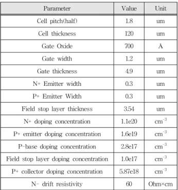
Table 3. Design Process Parameters of Final Device.
표 3. 최종소자 설계 공정변수
Parameter Value Unit
Cell pitch(half) 1.8 um
Cell thickness 120 um
Gate Oxide 700 Å
Gate width 1.2 um
Gate thickness 4.9 um
N+ Emitter width 0.3 um
P+ Emitter Width 0.3 um
Field stop layer thickness 3.54 um N+ doping concentration 1.1e20 cm
-3P+ emitter doping concentration 1.6e19 cm
-3P-base doping concentration 2.8e17 cm
-3Field stop layer doping concentration 1.0e17 cm
-3P+ collector doping concentration 5.87e18 cm
-3N- drift resistivity 60 Ohm×cm
최종 설계한 FS-IGBT의 항복전압과 Switching 특성은 그림 9와 10에 나타내었고, 최종소자 설계 의 공정 변수는 표 3에 나타내었다.
Ⅳ. 결론
Gate Oxide Thickness 증가에 따라 Eon과 VCE-SAT
이 증가하였고, Eoff의 특성이 감소하는 경향을 보 였다. 이러한 Trade-off 관계를 고려하여 Gate Oxide Thickness는 700Å일 때 가장 좋은 특성을 가졌다.
P+ Emitter Width는 0.3um 이하에서 우수한 전 기적 특성을 가졌고, Trench Gate width는 증가할 수록 특성이 향상되었다. 이는 단위 Cell의 크기를 최소화하면서 Trench Gate width는 공정이 허용하 는 범위에서 넓게 설계하는 것이 스위칭 특성에서 유리한 것으로 판단된다.
하지만 Trench Gate width가 증가하면 Cell Pitch의 증가로 인해 웨이퍼당 순수 소자의 수가감 소하기 때문에 생산비용을 고려하여 소형화가 필 요하다.
Synopsys T-CAD Simulator를 통해 1,200V급 IGBT의 마진율을 고려한 항복전압 1,470V와 VCE-SAT
2.17V, Eon 0.361mJ, Eoff 1.152mJ의 전기적 특성 을 갖는 IGBT 소자를 구현하였다.
References
[1] B. S. Ann, “A study on 1200V high efficiency field stop IGBT,” Ph.D diss, Far East University, 2018.
[2] Baliga, B. Jayant, “The IGBT device: physics, design and applications of the insulated gate bipolar transistor,” William Andrew, 2015.
[3] E. G. Kang, “Design and Analyzing of Electrical Characteristics of 1,200 V Class Trench Si IGBT with Small Cell Pitch,” Journal of the Korean
Institute of Electrical and Electronic Material Engineers Vol.33, No.2, pp.105-108, 2020.
DOI: 10.4313/JKEM.2020.33.2.105
[4] E. G. Kang, “Design of 1,200 V Class High Efficiency Trench Gate Field Stop IGBT with Nano Trench Gate Structure,” Journal of the
Korean Institute of Electrical and Electronic Material Engineers, Vol31, no.4, pp.208-211,
2018. DOI: 10.4313/JKEM.2018.31.4.208[5] Laska, T., M. Munzer, F. Pfirsch, C. Schaeffer, and T. Schmidt, “The field stop IGBT (FS IGBT).
A new power device concept with a great improvement potential,” In 12th International
Symposium on Power Semiconductor Devices &
ICs. Proceedings (Cat. No. 00CH37094), IEEE,
pp.355-358, 2000. DOI: 10.1109/ISPSD.2000.856842 [6] E. G. Kang, “A Study Comparison and Analysis of Electrical Characteristics of IGBTs with Variety Gate Structures,” Journal of the Korean Instituteof Electrical and Electronic Material Engineers,
Vol.29. No.11, pp.681-684, 2016.DOI: 10.4313/JKEM.2016.29.11.681
[7] Shin, Samuell, et al. “2500V IGBTs with Low on Resistance and Faster Switching Characteristic,”
Journal of IKEEE, Vol.12. No.2, pp.110-117,
2008.BIOGRAPHY