1. INTRODUCTION
Hydrogenated amorphous silicon (a-Si:H) is tremendously used for various industrial applications such as thin film transistors (TFTs) for liquid crystal display (LCD), and optoelectronic devices like a thin film solar cells [1].
However, a-Si:H is required to improve the film quality because of low crystallinity and optical defect originated from localized states in the middle of bandgap [2].
Especially, a-Si:H has a low light absorption performance
a. Corresponding author; [email protected] Copyright ©2018 KIEEME. All rights reserved.
This is an Open-Access article distributed under the terms of the Creative Commons Attribution Non-Commercial License (http://creativecommons.org/licenses/by-nc/3.0) which permits unrestricted non-commercial use, distribution, and reproduction in any medium, provided the original work is properly cited.
in the infrared wavelength that is unsuitable for many applications [3]. One way to solve the optical problems is what choose the microcrystalline Si (μc-Si) instead of a-Si:H due to high photovoltaic quality [4]. Several microcrystalline silicon studies have been proposed in order to overcome these problems and use in various applications [5,6].
From previous report [7], the bandgap of active films can be controlled by alloying Ge with Si. With the increase of Ge concentrations, the band gap of SiGe film becomes narrower. It is well-known that microcrystalline SiGe thin films are studied for potential candidates for electric and optoelectronic applications [8,9]. For synthesis microcrystalline SiGe film, chemical vapor deposition has many advantages. Especially, the remote technique has an
원격 플라즈마 화학기상 증착법으로 성장된 미세 결정화된 SiGe 박막 형성
김도영a
울산과학대학교 전기전자공학부
The Formation of Microcrystalline SiGe Film Using a Remote Plasma Enhanced Chemical Vapor Deposition
Doyoung Kima
School of Electrical and Electronics Engineering, Ulsan College, Ulsan 44022, Korea
(Received May 7, 2018; Revised May 17, 2018; Accepted May 18, 2018)
Abstract: SiGe thin films were deposited by remote plasma enhanced chemical vapor deposition (RPE-CVD) at 400℃ using SiH4 or SiCl4 and GeCl4 as the source of Si and Ge, respectively. The growth rate and the degree of crystallinity of the fabricated films were characterized by scanning electron microscopy and Raman analysis, respectively. The optical and electrical properties of SiGe films fabricated using SiCl4 and SiH4 source were comparatively studied. SiGe films deposited using SiCl4 source showed a lower growth rate and higher crystallinity than those deposited using SiH4 source. Ultraviolet and visible spectroscopy measurement showed that the optical band gap of SiGe is in the range of 0.88~1.22 eV.
Keywords: Silicon germanium, Silicon chloride, Silane, Germanium chloride, Raman spectroscopy, Optical bandgap
Regular Paper 320
J. Korean Inst. Electr. Electron. Mater. Eng.
Vol. 31, No. 5, pp. 320-323 July 2018 DOI: https://doi.org/10.4313/JKEM.2018.31.5.320 ISSN 1226-7945(Print), 2288-3258(Online)
전기전자재료학회논문지, 제31권 제5호 pp. 320-323, 2018년 7월: 김도영 321
inherent advantage of no direct exposure to the plasma during the deposition process. This eliminates the damage to the film surface from energetic particles in the plasma.
In this paper, we performed the deposition and evaluations of microcrystalline SiGe films as a function of Ge concentrations using a remote plasma enhanced chemical vapor deposition (RPE-CVD). And we used two sources of SiH4 and SiCl4 for Si source. They were comparatively studied with GeCl4 as Ge source. The growth characteristics and the electrical properties and the optical transmittance spectra of SiGe film were discussed too.
2. METHOD FOR EXPERIMENT
In this experiment, the SiGe films were deposited by RPE-CVD method. This equipment consisted of chamber and cylindrical cavity connected with RF power generator to create plasma away from the samples.
Maximum 8 inch sample can be loaded and the vacuum of the chamber was set by low vacuum pump and the base pressure is 30 mTorr. Hydrogen gas for plasma was passed through the cavity directed to the sample holder and its flow was kept to 70 sccm by mass flow controller. The source synthesized SiGe film was used the chemical of SiCl4, GeCl4, and the gas of SiH4. In order to control the flow rate of sources, the needle valve was applied without bubbling because of their enough vapor pressure at room temperature. With these flow, the chamber pressure increased to about 10 mTorr at standard growth condition. The temperature of gas lines were maintained higher than source canister for prevent of the chemical source condensation. The corning glass was used for substrate, and RF power and deposition temperature and time were fixed to 300 W, 400℃ and 20 min, respectively.
The microstructure and structural properties of SiGe films were analyzed by SEM (JSM-6700F), and Raman spectroscopy (LabRam HR, Ar-ion laser, 514 nm). Also the changes in SiGe optical band gap and film resistivity depending on Ge concentration were studied using UV-VIS (PerkinElmer Inc., Lambda 35) and Hall effect measurement (Eopia HEM-2000), respectively.
3. RESULTS AND DISCUSSIONS
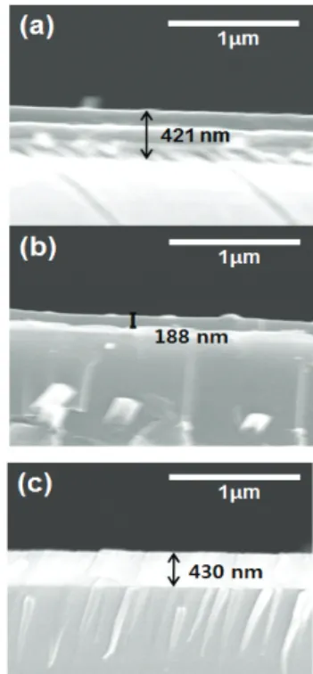
SiGe film was deposited at 400℃ with the environment of H2 plasma. The sources of SiGe are used SiH4 with GeCl4 and SiCl4 with GeCl4, respectively. When chemical and source gas supplied to the chamber, the base pressure maintained 40 mTorr. The partial pressure of SiH4 and SiCl4 fixed 30 mTorr. That of GeCl4 fixed as 10 mTorr. Figure 1 exhibited vertical images of SiGe films using a SEM. In using a SiH4 and GeCl4 of Fig.
1(a), SiGe film was deposited 421 nm with the growth rate of 30.5 nm/s. In using a SiCl4 and GeCl4 of Fig.
1(b), SiGe film was deposited 188 nm with growth rate of 10.6 nm/s. Single Ge film without Si source was deposited 430 nm (growth rate = 30.6 nm/s) as shown Fig. 1(c). In this case, Cl atom also has an influence on reduce the growth rate of SiGe film. From SEM observation, the Cl has larger binding energy with Ge (390.8 kcal/mol) than hydrogen (263.2 kcal/mol). Although the decomposition energy of chlorine on the Ge surface is not reported yet, large binding energy of Cl had a big
Fig. 1. SEM image of SiGe films with H2 plasma at 400˚C : (a) using SiH4 and GeCl4, (b) using SiCl4 and GeCl4, and (c) using only GeCl4.
J. Korean Inst. Electr. Electron. Mater. Eng., Vol. 31, No. 5, pp. 320-323, July 2018: D. Kim 322
influence on the suppression of chlorine decomposition on SiGe film surface. Therefore, additional Cl passivation effects to decrease the growth rate of films deposited by SiCl4 and GeCl4.
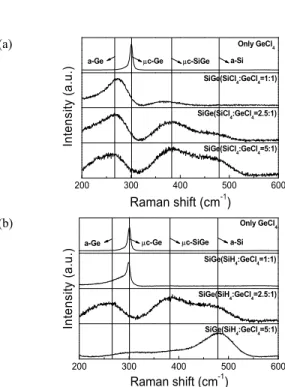
SiGe films were deposited as a function of Si and Ge partial gas pressure rate from 1:1 to 5:1 to same working pressure of 40 mTorr. Figure 2 shows the change of Raman spectra of SiGe films. In Fig. 2(a), the narrow peak located at 300 cm-1 shows crystalline structure of Ge film deposited by only GeCl4 without any Si source. However, with increasing rate of SiCl4
source, the intensity of Ge peak is decreased due to the increasing of Ge amorphous phase. And additional peaks appear at around 380 and 480 cm-1 due to Si-Ge and Si-Si bonds [10]. When the rate of partial gas pressure is 1:1, the film is still formed amorphous Ge film although crystallization is suppressed by Si atoms. With increasing the partial pressure of Si source, the peak intensity of Ge-Ge band decreases and that of Si-Si band increases.
This means the formation of microcrystalline SiGe films at the condition of the rate of SiCl4 and GeCl4 of 5:1.
SiGe was also deposited by a SiH4 and GeCl4 source as shown in Fig. 2(b). The peak of Ge-Ge was strongly
dominant at around 300 cm-1 when the rate of SiH4 and GeCl4 is 1:1. This means Ge film doped Si is formed because of low SiH4 source concentration. Ge film has high crystallinity because the peak is little shifted to the low frequency and low full width half maximum. The SiGe film was formed as an increasing rate of Si partial gas pressure, but the peaks of SiGe disappeared when the rate of SiH4 and GeCl4 is 5:1. It expects the most of Si film is formed high SiH4 gas partial pressure because of higher decomposition rate of SiH4 gas than GeCl4 source.
The optical properties of SiGe films were measured by ultraviolet-visible (UV-VIS) wavelength spectroscopy.
From these results, the optical band gap (Eg) could be calculated using a following equation [11]:
(1)
Where α is the absorption coefficient, h is Plank’s constant, γ is the photon frequency, A is a constant, respectively. The values of (αhγ)1/2 were plotted as a function of photon energy (hγ) as shown in Fig. 3, and then Eg can be determined by extrapolation of the linear part. The optical band gap was evaluated to be 1.05, 1.22 eV for SiGe films deposited to be used SiCl4 source and to be used SiH4, respectively. From this results, we could (a)
Raman shift (cm-1)
Intensity (a.u.)
200 300 400 500 600
SiGe(SiCl4:GeCl4=1:1)
SiGe(SiCl4:GeCl4=5:1) SiGe(SiCl4:GeCl4=2.5:1) Only GeCl4
c-Ge
a-Ge c-SiGe a-Si
(b)
a-Si
c-SiGe
c-Ge
Only GeCl4
Raman shift (cm-1) Intensity (a.u.) a-Ge SiGe(SiH
4:GeCl4=1:1)
SiGe(SiH4:GeCl4=2.5:1)
SiGe(SiH4:GeCl4=5:1)
200 300 400 500 600
Fig. 2. Raman spectra of Si films deposited as a function of (a) the rate of partial gas pressure of SiCl4 and GeCl4 and (b) the rate of partial gas pressure of SiH4 and GeCl4.
0.5 1.0 1.5 2.0 2.5 3.0
2 4 6 8 10
used SiCl4 Eg= 1.05 eV used SiH4 Eg= 1.22 eV
h (x102 cm-1 eV)1/2
Photon energy (eV) (a)
0.5 1.0 1.5 2.0 2.5 3.0
2 4 6 8
only GeCl4 Eg= 0.88 eV
h (x102 cm-1 eV)1/2
Photon energy (eV) (b)
Fig. 3. Optical band gap of (a) SiGe films and (b) only Ge film by GeCl4.
전기전자재료학회논문지, 제31권 제5호 pp. 320-323, 2018년 7월: 김도영 323
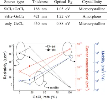
know that the SiGe film used SiCl4 was more cooperated with Ge than that used SiH4 because the Eg of only Ge is lower than SiGe. That value using only GeCl4 was 0.88 eV. This result supports that the optical Eg of Ge film is lower than SiGe film. We summarized physical and optical performances as a function of Si and Ge source as shown in Table 1.
In order to evaluate the electrical performance of the SiGe film as a function of GeCl4 rate, we tried the Hall effect measurement as shown in Fig. 4. As increasing of input GeCl4 rate, carrier concentration and mobility was increased simultaneously. Above these results, resistivity was decreased. However, the resistivity of film used SiCl4
as the Si source was faster decreased than the case of SiH4. This result might be considered that SiGe film used SiCl4 source had a lower defects than used SiH4.
4. CONCLUSION
Microcrystalline SiGe films were deposited by remote plasma enhanced chemical vapor deposition with several
GeCl4 concentrations and two Si sources of SiCl4 and SiH4. The crystallinity of SiGe films deposited to be used SiCl4 source had better than SiH4 source with low GeCl4
concentration condition. The optical band gap of SiGe films was lower than that of Si and it can be changed with incorporation of SiCl4 and SiH4 source. The electrical properties of SiGe showed the resistivity was decreased with GeCl4 source concentrations.
REFERENCES
[1] H. Meiling and R.E.I. Schropp, Appl. Phys. Lett., 70, 2681 (1987). [DOI: https://doi.org/10.1063/1.118992]
[2] R. A. Street, D. K. Biegelsen, and J. C. Knights, Phys. Rev. B, 24, 969 (1981). [DOI: https://doi.org/10.1103/PhysRevB.24.969]
[3] O. Vetterl, F. Finger, R. Carius, P. Hapke, L. Houben, O.
Kluth, A. Lambertz, A. Mück, B. Rech, and H. Wagner, Sol.
Energy Mater. Sol. Cells, 62, 97 (2000). [DOI: https://doi.org/
10.1016/S0927-0248(99)00140-3]
[4] M. Faraji, S. Gokhale, S. M. Choudhari, and M. G. Takwale, Appl. Phys. Lett., 60, 3289 (1992). [DOI: https://doi.org/10.1063/
1.106722]
[5] Z. Huang, J. E. Carey, M. Liu, X. Guo, E. Mazur, and J. C.
Campbell, Appl. Phys. Lett., 89, 033506 (2006). [DOI: https://
doi.org/10.1063/1.2227629]
[6] K. Ishizaki, A. Motohira, M. De Zoysa, Y. Tanaka, T. Umeda, and S. Noda, IEEE J. Photovoltaics, 7, 950 (2017). [DOI:
https://doi.org/10.1109/JPHOTOV.2017.2695524]
[7] G. H. Wang, C. Y. Shi, L. Zhao, H. W. Diao, and W. J.
Wang, J. Alloys Compd., 658, 543 (2016). [DOI: https://
doi.org/10.1016/j.jallcom.2015.10.235]
[8] A. S. Gudovskikh, A. V. Uvarov, I. A. Morozov, A. I. Baranov, D. A. Kudryashov, K. S. Zelentsov, A. S. Bukatin, and K.
P. Kotlyar, J. Vac. Sci. Technol., A, 36, 02D408 (2018).
[DOI: https://doi.org/10.1116/1.5018259]
[9] X. Zhao, D. Li, T. Zhang, B. Conrad, L. Wang, A. H. Soeriyadi, J. Han, M. Diaz, A. Lochtefeld, A. Gerger, I. Perez-Wurfl, and A. Barnett, Sol. Energy Mater. Sol. Cells, 159, 86 (2017). [DOI:
https://doi.org/10.1016/j.solmat.2016.08.037]
[10] A. Fedala, C. Simon, N. Coulon, T. Mohammed-Brahim, M.
Abdeslam, and A. C. Chami, Phys. Status Solidi C, 7, 762 (2010). [DOI: https://doi.org/10.1002/pssc.200982791]
[11] M. Beaudoin, M. Meunier, and C. J. Arsenault, Phys. Rev.
B, 47, 2197 (1993). [DOI: https://doi.org/10.1103/PhysRevB.
47.2197]
Source type Thickness Optical Eg Crystallinity SiCl4+GeCl4 188 nm 1.05 eV Microcrystalline SiH4+GeCl4 421 nm 1.22 eV Amorphous only GeCl4 430 nm 0.88 eV Microcrystalline Table 1. Summary of physical and optical performances as a function of Si and Ge source.
Fig. 4. Electrical performance of SiGe film (a) using SiH4 and GeCl4 and (b) using SiCl4 and GeCl4 by Hall measurement.