Enhancement in the photocurrent of ZnO nanoparticles by thermal annealing
Kwangsub Byun
*, Kyuongah Cho
*, Jin Hyung Jun
*, Hojun Seong
*and Sangsig Kim
*,★
Abstract
The optoelectrical characteristics of the ZnO nanoparticles (NPs) annealed in vacuum or oxygen condition from 200 oC to 600 oC were examined. Increased on-off ratio (or, the ratio of photocurrent to dark current) was observed when they were annealed at 300 oC, 400 oC and 500 oC with the values enhanced about 4 orders compared to the as-prepared ZnO NPs in both annealing conditions, while the maximum efficiency was shown at the annealing temperature of 600 oC for the ZnO NPs annealed in vacuum with the value of 29.8 mA/W and at the temperature of 500 oC for those annealed in oxygen condition with the value of 40.3 mA/W.
Photoresponse behavior of the ZnO NPs annealed in oxygen showed the sharp increase right after the ir exposure to the light followed by the slow decay and saturation during steady illumination, differing from the ZnO NPs annealed in vacuum which only exhibited the gradual increase. This difference occurred due to the curing effect of the oxygen vacancies. SEM images indicated no change in their morphologies with annealing, indicating the change in their internal structures by annealing, and most remarkably at 600 oC. As for their photoluminescence(PL) spectra, the decrease of the deep-level(DL) emission was observed when they were annealed in oxygen at 400 oC, and not at 200oC and 600 oC.
Key words: Optoelectrical characteristic, Zinc oxide nanoparticle, Annealing, Photoresponse
* Dept. of Electrical Engineering and Institute for Nano Science, Korea University
★Corresponding author
※ Acknowledgment
This work was supported by the Center for Integrated-Nano-Systems (CINS) of the Korea Research Foundation (KRF-2006-005-J03601), the Medium-term Strategic Technology Development Program, and the "SystemIC2010" project of the Korea Ministry of Commerce, Industry and Energy, the Korea Science and Engineering Foundation (KOSEF) through the National Research Lab. Program (R0A-2005-000-10045-0 (2008)), the Nano R&D Program (M10703000980-08M0300-98010), and World Class University (WCU, R32-2008-000-10082 -0) Project of the Ministry of Education, Science and Technology.
Manuscript received Mar. 4, 2009 ; revised Mar.29, 2009
I. Introduction
ZnO has been a center of attention as a very
useful material for UV detection with its beneficial characteristics such as large binding energy (60 meV) and wide band gap (3.37 eV) [1-6]. Its performance as UV detector is known to improve when oxygen molecules are adsorbed onto its surface, because desorption of the chemiadsorbed oxygen ions under illumination allows the electrons that were taken by the adsorbed oxygen to be released and deplete the holes created from electron-hole pairs generated by illumination [7-9].
Meanwhile, many studies were performed on the effect of annealing temperature and ambient condition for ZnO [10-13]. These results revealed that annealing of ZnO produces more vacancies on the surface as well as in the inner part with their density varying depending on annealing temperature.
Therefore, when ZnO is annealed in oxygen condition, the increased number of oxygen is adsorbed on its surface and have more defects filled up inside. These results give the clue on how to
-3 -2 -1 0 1 2 3 -6
-4 -2 0 2 4 6
Current (μA)
Voltage (V) Dark current
Photocurrent
34.4 29.8
4.51x10⁴ 2.75x10²
600
40.3 13.5
9.98x10⁵ 2.24x10⁶ 500
16.5 8.74
1.23x10⁶ 6.53x10⁵ 400
8.1 4.96 1.87x10⁶ 2.39x10⁶ 300
4.27 2.24
1.44x10⁴ 0.33x10⁴
200
oxygen vacuum oxygen
vacuum
ambient
Temperature
efficiency on-off ratio
34.4 29.8
4.51x10⁴ 2.75x10²
600 oC
40.3 13.5
9.98x10⁵ 2.24x10⁶ 500 oC
16.5 8.74
1.23x10⁶ 6.53x10⁵ 400 oC
8.1 4.96 1.87x10⁶ 2.39x10⁶ 300 oC
4.27 2.24
1.44x10⁴ 0.33x10⁴
200 oC
oxygen vacuum oxygen
vacuum
ambient
Temperature
efficiency on-off ratio
34.4 29.8
4.51x10⁴ 2.75x10²
600
40.3 13.5
9.98x10⁵ 2.24x10⁶ 500
16.5 8.74
1.23x10⁶ 6.53x10⁵ 400
8.1 4.96 1.87x10⁶ 2.39x10⁶ 300
4.27 2.24
1.44x10⁴ 0.33x10⁴
200
oxygen vacuum oxygen
vacuum
ambient
Temperature
efficiency on-off ratio
34.4 29.8
4.51x10⁴ 2.75x10²
600 oC
40.3 13.5
9.98x10⁵ 2.24x10⁶ 500 oC
16.5 8.74
1.23x10⁶ 6.53x10⁵ 400 oC
8.1 4.96 1.87x10⁶ 2.39x10⁶ 300 oC
4.27 2.24
1.44x10⁴ 0.33x10⁴
200 oC
oxygen vacuum oxygen
vacuum
ambient
Temperature
efficiency on-off ratio
maximize its characteristics to be used as UV detection. Despite this fact, not many studies focused on examining their optoelectrical characteristics with different annealing conditions in oxygen condition. In this study, we examined the optoelectrical characteristics of ZnO annealed in oxygen condition and compared to the ZnO annealed in vacuum to observe the effect of annealing temperature. As for its dimension, NPs were used because they were expected to produce more favorable results for UV detection with a large on-off ratio or the improved absorption of light.
II. Experimental
Gold electrodes separated by 20 μm were patterned by photolithography and thermal evaporation on a Si substrate. 1 g of ZnO NPs (purchased from Sigma Aldrich co.) with an average diameter of 70 nm was dispersed in 20 ml methanol to be cast between the electrodes. Samples were annealed for 1 h in vacuum or oxygen at the various temperatures from 200 oC to 600 oC. Photocurrent, photoresponse and PL were measured at room temperature in air.
The light source for photocurrent, photoresponse and PL spectra was the He-Cd laser of the 325 nm wavelength with the optical power of 10 mW, and photocurrent and photoresponse were detected by an Agilent 4155C semiconductor parameter analyzer while PL intensities were recorded by an InGaAs detector equipped with a monochromator (SPEX 1000M).
III. Results and Discussion
Figure 1 shows the photocurrent characteristics of the as-prepared ZnO NPs. The I-V characteristics of the dark current and photocurrent are both ohmic. The on-off ratio and efficiency are 1.94 x 10² and 0.49 mA/W at 2.5 V.
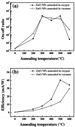
The on-off ratio and efficiency of the ZnO NPs annealed at various temperatures in vacuum or oxygen condition are presented in Table. 1 and plotted in Fig. 2. We observe in Fig. 2(a) that the on-off ratio is larger when ZnO NPs are annealed at 300 oC, 400 oC, 500 oC in both annealing conditions with their values increasing from 6.53 x
Fig. 1. Dark current and photocurrent (excited by the 325 nm wavelength light) plotted as a function of the applied voltage for the ZnO NPs.
Table 1. The ratio of the photocurrent to the dark current (or, on-off ratio) and efficiency of the annealed ZnO NPs in vacuum and oxygen under the illumination of light with the 325 nm wavelength.
105 to 2.24 x 10⁶ times that of the as prepared ZnO NPs while it is relatively smaller for the ZnO NPs annealed at 200 oC and 600 oC. The reduction of the on-off ratio when annealed at 600 oC is due to the sudden increase of the dark current. On the other hand, the efficiency is calculated to be maximum at the annealing temperature of 600 oC with the value at 29.8 mA/W when ZnO NPs are annealed in vacuum, and in case of annealing in oxygen, the magnitude is largest with 40.3 mA/W at 500 oC.
The efficiency tends to improve as the annealing temperature increases in vacuum condition, but when they was annealed in oxygen, this tendency is changed with its largest value at the annealing
0 100 200 300 400 500 600 102
103 104 105 106 107 108
(a)
ZnO NPs annealed in oxygen ZnO NPs annealed in vacuumOn-off ratio
Annealing temperature(°C)
0 100 200 300 400 500 600
0 10 20 30 40 50
(b)
Efficiency (mA/W)
Annealing temperature (°C)
ZnO NPs annealed in oxygen ZnO NPs annealed in vacuum
0 100 200 300 400 500 600
102 103 104 105 106 107 108
(a)
ZnO NPs annealed in oxygen ZnO NPs annealed in vacuumOn-off ratio
Annealing temperature(°C)
0 100 200 300 400 500 600
0 10 20 30 40 50
(b)
Efficiency (mA/W)
Annealing temperature (°C)
ZnO NPs annealed in oxygen ZnO NPs annealed in vacuum
Fig. 2. (a) On-off ratio and (b) efficiency of the ZnO NPs plotted as a function of the annealing temperature under the illumination of 325 nm light at a bias voltage of 2.5 V.
temperature of 500 oC and the value decreasing at the higher annealing temperature of 600 oC.
The annealing effect on the photocurrent of the ZnO NPs is related to the oxygen vacancies on the surface. When the oxygen vacancies increase on the surface, more oxygen molecules in air are supposed to adsorb on them, contributing to the increase of the photocurrent. The relation between the density of the surface oxygen vacancies and annealing temperature has been examined in a few reports [14-15]. They reported that the annealing treatment of ZnO at the temperatures higher than 300 oC leads to the remarkable increase of water adsorption into ZnO with the strikingly reduced angle of the water drops on the surface. Considering that both
water and oxygen molecules have the tendency to coordinate into the oxygen defect sites, this result is applicable to oxygen molecules. The similar result was reported for TiO2 on which the water absorption increase was spotted at the higher temperature than 227oC. From these results, the critical temperature that brings the noticeable change on the surface of ZnO and TiO2 is noticed between 200oC and 300oC and the effect became severe with increasing annealing temperature. In this study,we observe that the on-off ratio becomes very large at the annealing temperature of 300 oC, 400 oC and 500 oC averaging an increase of 4 orders from the as prepared ZnO NPs, and also the efficiency values increase compared to the as prepared ZnO NPs. This result is in very good agreement of the references [14-15] which mentioned the increase of surface vacancy effect at the higher annealing temperature than 300 oC and this is also supported by the smaller magnitude of the on-off ratio at the annealing temperature of 200
oC that was caused by the insufficient thermal energy at the temperature.
As for the annealing temperature of 600 oC, the efficiency decreases compared to those annealed at 500 oC for the ZnO NPs in case of the oxygen annealing condition, while that of the ZnONPs annealed in vacuum still increases. Therefore, the difference of the efficiencies between the ZnO NPs annealed on vacuum and oxygen is reduced at 600oC, showing a very little gap between them. The increase of the XRD peak along the c-axis (0002) is known to be remarkably enhanced with the higher annealing temperature than 600 oC, so that along with the increase of the dark current when annealed at 600 oC shown above, it can be possibly assumed that annealing of ZnO NPs at 600 oC possibly brings the change to the optoelectrical characteristics of the ZnO NPs. This characteristic was cautiously observed for the other experiments shown below.
Figure 3 presents the photoresponse of the ZnO NPs annealed at (a) 200 oC, (b) 400 oC and (c) 600
oC as a function of time at a bias voltage of 1 V.
It is notable that the large difference is shown between the ZnO NPs annealed in vacuum and oxygen at 400 oC, differently from the ZnO NPs
0 100 200 300 400 500 600 0
20 40 60 80 100 120 140 160
as-prepared
annealed in vacuum at 600 °C annealed in oxygen at 600 °C
Current (μA)
Time (sec)
on off on off
on off
× 20
(c)
0 10 20 30 40 50 60 70 80
× 5
× 10 as-prepared
annealed in vacuum at 400 °C annealed in oxygen at 400 °C
Current (μA) off off
on on on
off
(b)
0 2 4 6 8 10 12 14
16 as-prepared
annealed in vacuum at 200 °C annealed in oxygen at 200 °C
on off off on
on
Current (μA) off
(a)
Fig. 3. Magnitudes of the photocurrent plotted as a function of time when the light with the wavelength of 325 nm was switched on and off at the bias of 1 V to the ZnO NPs annealed at (a) 200 oC, (b) 400
oC and (c) 600 oC in different ambient conditions.
annealed at 200 oC that exhibited the ignorable difference between the ZnO NPs annealed in two conditions. The result shows the thermal energy effect mentioned in Table. 1and Fig. 2.
The photocurrent of the ZnO NPs annealed in vacuum exhibits the steady increase as time passes by just as the as prepared ZnO NPs. This behavior matches the usually known characteristic of ZnO.
The steady increase of the photocurrent under
illumination has been revealed to be mainly concerned with trap sites; i.e, when some electrons fall into the trap sites formed by oxygen vacancies, they either recombine with the photo-generated holes or are detrapped back to the conduction band by overcoming the energy barrier. The increase of the photocurrent is explained by the dominance of the electrons that overcome the barrier over the ones that recombine. Thus, this behavior of the ZnO NPs annealed in vacuum is understandable considering its nature to produce oxygen vacancies.
On the other hand, ZnO NPs annealed in oxygen shows the sharp increase of the current right after they are exposed to the light and the slow decay and saturation afterwards. This behavior is a unique characteristic distinguished from the ZnO NPs annealed in vacuum and from this fact, it is induced that this behavior is due to the curing effect of oxygen. The curing of those vacancies reduces the number of trap sites the electrons fall into, and this increases their lifetime. Owing to this increased lifetime, the density of charge carriers increases and the photocurrent improves. This effect is severe and the initial magnitude of the photocurrent is so huge.
As for the gradual decay of the photocurrent after this sharp increase, there are some possible explanations but the most reasonable one is that some of oxygen are desorbed incompletely from the surface and readsorb onto the surface under illumination. These readsorbed oxygen molecules take the free electrons, leading to the decrease of the current.
In calculating the time constant, we took three stages of the photoresponse into account. The rising times for the ZnO NPs annealed in vaccum or oxygen are both within 1 s except the ZnO NPs annealed in oxygen at 600 oC, which shows the rise time constant τ=1.9 s. The decay time constants are divided into two stages, which are the fast decay process and the secondary subsequent process. The fast decay processes exhibits the decay time constants all within 1 s just as the rising times, and the subsequent decay times are 13.5 s, 2.8 s, 48.5 s for the ZnO NPs annealed at 200 oC, 400 oC and 600 oC in vacuum and 21 s, 4.5 s, 3.8 s for the ZnO NPs annealed at 200 oC, 400 oC and 600 oC in oxygen, respectably. The short response time for
PL (arb.)
as-prepared
annealed in vacuum 200 ° C annealed in oxygen 200 ° C
(a)
as-prepared
annealed in vacuum at 400 °C annealed in oxygen at 400 °C
(b)
PL (arb.)
350 400 450 500 550
as-prepared
annealed in vacuum at 600 °C annealed in oxygen at 600 °C
PL (arb.)
Wavelength (nm)
(c)
PL (arb.)
as-prepared
annealed in vacuum 200 ° C annealed in oxygen 200 ° C
(a)
as-prepared
annealed in vacuum at 400 °C annealed in oxygen at 400 °C
(b)
PL (arb.)
350 400 450 500 550
as-prepared
annealed in vacuum at 600 °C annealed in oxygen at 600 °C
PL (arb.)
Wavelength (nm)
(c)
the rise and decay time is due to the generation and recombination of the electron-hole pairs and the slow secondary decay time is caused by the readsorption of the oxygen molecules. It was reported that the longer subsequent decay time is induced by the reduced rate of the oxygen readsorption onto the surface of ZnO, which usually occurs when the surface coverage rate is so high [16]. ZnO NPs annealed in vacuum have more vacancies on their surfaces than the ZnO NPs annealed in oxygen, so that the subsequent decay time is reduced for them when the light is switched off.
The SEM images for the ZnO NPs annealed at 200 oC, 400 oC and 600 oC are displayed in Fig. 4.
These images indicate that there is almost no change in their morphologies at all the annealing temperatures. This indicates that the change in their optoelectrical characteristics is mostly concerned with the change in their internal structures instead of the interaction between the particles. To examine this further, we investigated the PL spectra of the ZnO NPs.
500nm
(a)
(c) (d)
(b)
500nm 500nm
500nm 500nm
(a)
(c) (d)
(b)
500nm 500nm
500nm
Fig. 4. SEM images of the ZnO NPs (a) as prepared and annealed at (b) 200 oC,(c)400oC and (d) 600 oC in oxygen condition.
Figure 5 shows the PL spectra of the ZnO NPs as prepared and annealed at various temperatures in vacuum or oxygen condition. It is presented in Fig.
5(a) that the PL spectra of the as prepared, vacuum and oxygen annealed ZnO NPs exhibited an ignorable difference in their values when they were annealed at 200 oC, while the plunge of the deep-level(DL) emission at the wavelength of about
Fig. 5. PL spectra of the ZnO NPs when they were annealed at (a) 200 oC, (b) 400 oC and (c) 600 oC in different ambient conditions under the illumination of the light with the 325 nm wavelength.
450 nm appeared for the ZnO NPs annealed at 400
oC in oxygen in Fig. 5(b). This plunge of the DL emission peak has something to do with the increase of the oxygen vacancies on the surface and in the inner part by annealing, because the DL emission of ZnO is caused by the oxygen vacancies which have the wavelength at around 450 nm.
Thus, the peak at this wavelength decreases when
the vacancies are filled up. This result is in agreement with Fig. 2, showing the relation between the photocurrent and PL spectra. The curing of the oxygen vacancies leads to the increase of the photocurrent, so when the largest photocurrent is observed, the drop of the PL spectra at the wavelength of 450 nm is also largest. For the ZnO NPs annealed at 600 oC, the decrease of the DL peak was not shown differently from those of the ZnO NPs annealed at 400oC. The different optoelectrical characteristic was expected from Table 1. It suggests that annealing of ZnO at the high temperature reduces the curing effect of the defects even though it is done in oxygen condition, and from the result we obtained, this PL spectra behavior is assumedly concerned with the improvement of the crystalline.
IV. Summary
We have examined the photocurrent characteristics of the ZnO NPs annealed in vacuum or oxygen condition at the various annealing temperatures from 200 to 600 oC. The on-off ratio and efficiency are 1.94 x 10² and 0.49 mA/W for the as prepared ZnO NPs, respectably. The on-off ratios are enhanced from 6.53 x 10⁵ to 2.24 x 10⁶ times those of the as-prepared ZnO NPs at the annealing temperatures of 300 oC, 400 oC and 500 oC in both photoresponse, the ZnO NPs annealed in oxygen shows the sharp increase right after exposure to the light and gradual decrease and saturation process during the steady illumination, while the ZnO NPs as prepared and annealed in vacuum exhibits only the steady increase. This difference is due to the curing effect of the oxygen vacancies in oxygen condition. SEM images display no morphological change between particles, indicating the change in their internal structures. PL spectra shows the decrease of the deep–level peak when the ZnO NPs are annealed in oxygen at 400oC. At the annealing temperature of 600 oC, PL spectra exhibits the different tendency of their behavior and it is assumedly due to the improved crystalline at the temperature.
References
[1] W. C. T. Lee, M. Henseler, P. Miller, C. H.
Swartz, T. H. Myers, R. J. Reeves, and S. M.
Durbin, “Effect of annealing on the morphology and optoelectrical characteristics of ZnO thin films grown by plasma-assisted molecular beam epitaxy,”
J. of Elec. Mater., Vol. 35, pp.1316-1321, 2006 [2] Z. Y. Xue, D. H. Zhang, Q. P. Wang, and J. H.
Wang, “The blue photoluminescence emitted from ZnO films deposited on glass substrate by rf magnetron sputtering,” Appl. Surf. Sci., Vol.195, pp.126-129, 2002
[3] Z.-M. Liao, H.-Z. Zhang, Y.-B. Zhou, J. Xu, J.-M. Zhang, and D.- P. Yu, “Surface effects on photoluminescence of single ZnO nanowires,” Phys.
Lett. A, Vol.372, pp.4505-4509, 2008
[4] Z. Z. Zhi, Y. Qi, H. Z. Yang, J. H. Wang, X. M.
Yu, and B. S. Zhang, “Effects of annealing temperature on optical properties of ZnO nanocrystals embedded in SiO2 matrix thin films,” J.
Phys. D: Appl. Phys., Vol.40, pp.4281-4284, 2007 [5] K. S. Kim, H. W. Kim, and N. H. Kim,
“Structural characterization of ZnO films grown on SiO2 by the RF magnetron sputtering,” Physica B.
Vol.334, pp.343-346, 2003
[6] S. Liang, H. Sheng, Y. Liu, Z. Huo, Y. Lu, and H. Shen, “ZnO Schottky ultraviolet photodetectors,”
J. Cryst. Growth, Vol.225, pp.110-113, 2001
[7] X.G. Zheng, Q. S. Li, W. Hu, D. Chen, N.
Zhang, M. J. Shi, J. J. Wang, and L. C. Zhang,
“Photoconductive properties of ZnO thin films grown by pulsed laser deposition,” J. Lumin.. Vol.122, pp.198-201, 2007
[8] Y. Takahashi, M. Kanamori, A. Kondoh, H.
Minoura, Y. Ohya, “Photoconductivity of ultrathin zinc oxide films,” Jpn. J. Appl. Phys., Vol.33, pp.6611-6615, 1994
[9] W. H. Hirschwald, “Zinc oxide: an outstanding example of a binary compound semiconductor,” Acc.
Chem. Res., Vol.18, pp.228-234, 1985
[10] P. Sagar, P. K. Shishodia, R. M. Mehra, H.
Okada, A. Wakahara, and A. Yoshida,
“Photoluminescence and absorption in sol-gel-derived ZnO films,” J. Lumin,. Vol.126, pp.800-806, 2007
[11] H. S. Kang, J. S. Kang, J. W. Kim, and S. Y.
Lee, “Annealing effect on the property of ultraviolet and green emissions of ZnO thin films,” J. Appl.
Phys., Vol.95, pp.1246-1250, 2004
[12] X. M. Fan, J. S. Lian, Z. X. Guo, L. Zhao, and Q. Jiang, “Influence of the annealing temperature on violet emission of ZnO films obtained by oxidation of Zn film on quartz glass,” J. Mater. Sci., Vol.41, pp.2237-2241, 2006
[13] L. Chen, Z. Q. Chen, X. Z. Shang, C. Liu, S.
Xu, and Q. Fu, “Effect of annealing temperature on density of ZnO quantum dots,” Solid State Commun., Vol.137, pp.561-565, 2006
[14] R.-D. Sun, A. Nakajima, A. Fujishima, T.
Watanabe, and K. Hashimoto, “Photoinduced surface wettability conversion of ZnO and TiO2thinfilms,” J.
Phys. Chem. B, Vol.105, pp.1984-1990, 2001
[15] G. Lu, A. Linsebigler, J. T. Yates Jr.,
“Photooxidation of CH3Cl on TiO2 (110): A mechanism not involving H2O,” J. Phys. Chem., Vol.99, pp.7626-7631, 1995
[16] K. Keem, J. Kang, D.-Y. Jeong, B. Min, K.
Cho, H. Kim, S. Kim, and Y. K. Kim, “Aging effect on the optoelectronic properties of a single ZnO nanowire,” Jpn. J. Appl. Phys., Vol.46, pp.4355-4358, 2007
BIOGRAPHY
Byun Kwangsub (Student member)
2006 : BS degree in Electrical Engineering, Korea University.
Present : MS course in Electrical Engineering, Korea University
<Research Interests>
Fabrication of devices based on nano-particles
Cho Kyoungah (Non Member)
2000 : Ph.D. degree in Chemistry, Tokyo University.
Present : Research Professor, Institiute for Nano Science, Korea University
<Research Interests>
Electronic devices based on nano-particles
Jun Jin Hyung (Non Member)
2007 : Ph. D. degree in Advanced Materials Science and Engineering, Yonsei University.
Present : Research Professor, BK21 Division of Information Technology, Korea University
<Research Interests>
TFT devices based on nano-particles
Seong Hojun (Non Member)
2007 : BS degree in Electrical Engineering, Korea University.
Present : MS course in Electrical Engineering, Korea University.
<Research Interests>
Nano-hybrid optoelectronic devices
Kim Sangsig (Member)
1996 : Ph.D. degree in Semiconductor Physics, Colombia University.
1996-1998 : Post Doc., University of Illinois at Urbana-Champaign.
1998-1999 : Senior Researcher, University of Illinois at Urbana-Champaign.
Present : Professor, Dept. of Electrical Engineering, Korea University.
<Research Interests>
Electronic devices based on nano-particles and nano-wires