SiC based Technology for High Power Electronics and Packaging Applications
Ashutosh Sharma, Soon Jae Lee, Young Joo Jang and Jae Pil Jung
†Department of Materials Science and Engineering, University of Seoul, Seoul 130-743, Korea
(Received June 11, 2014: Corrected June 23, 2014: Accepted June 25, 2014)
Abstract: Silicon has been most widely used semiconductor material for power electronic systems. However, Si-based power devices have attained their working limits and there are a lot of efforts for alternative Si-based power devices for better performance. Advances in power electronics have improved the efficiency, size, weight and materials cost. New wide band gap materials such as SiC have now been introduced for high power applications. SiC power devices have been evolved from lab scale to a viable alternative to Si electronics in high-efficiency and high-power density applications.
In this article, the potential impact of SiC devices for power applications will be discussed along with their Si counterpart in terms of higher switching performance, higher voltages and higher power density. The recent progress in the development of high voltage power semiconductor devices is reviewed. Future trends in device development and industrialization are also addressed.
Keywords: SiC, Packaging, Semiconductor, IGBT, JFET
1. Introduction
1.1. Wide Band Gap Semiconductors
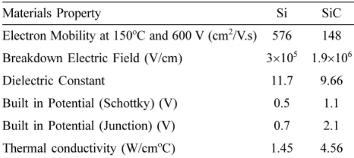
It has been already established that the major breakthrough in Power Electronics comes from the development and use of Wide Band Gap (WBG) semiconductor devices. Most commonly used WBG semiconductors in power electronics are as SiC, GaN, and diamond. WBG show superior material properties can be operated at higher switching speed, high voltage and high temperatures.
1)These unique properties provide a substantial change in their applications for power generation. The electrical power undergoes a number of conversion steps making the process highly inefficient, i.e., only 20% of the whole energy involved in energy generation reaches the end-user.
2)Thanks to the WGB semiconductors which increase the conversion efficiency due to their outstanding material properties.
The WBG semiconductors generally includes all materials with a band gap starting at roughly 2.0 eV, including indium nitride (InN) and cubic phase silicon carbide (3C-SiC), up to materials such as aluminum nitride (AlN) and diamond, which have energy gaps on the order of 6.0 eV. The electronic band gap of gallium arsenide (GaAs) at room temperature is about 1.42 eV. The most important features of a semiconductor with a large band gap are the sustainability
of a high breakdown voltage. It is generally believed that as the band gap increases, the breakdown voltage also increases accordingly. This is the most important advantage which enables the high voltage operation of devices. Moreover, the thermal leakage is drastically reduced, as compared to standard semiconductors. This allows devices to operate in high temperature environments or in systems where leakage current affects their performance, such as in photodetectors, charge-coupled devices (CCDs), and nonvolatile memories .
1, 2)1.2. SiC in Power Electronics
SiC is the potential reputed wide band gap semiconductor in advanced electronic applications Its unique properties allow the feasibility of easily growing a native oxide. The presence of numerous polytypes of SiC can potentially be used in a wide range of applications such as microwave and high-power devices. The use of SiC based devices is improving many aspects of current electronics due to the limitations of Si in region of high-frequency and high-power applications.
3-5)For example, in wireless communication, there is always a demand for microwave transistors capable of high power densities. In addition, the data storage and optical communication systems markets have developed high frequency emitters and detectors.
6)Therefore, the various transport properties and breakdown characteristics
†