碩士學位論文
대면적, 고화질 TFT/LCD's 적용을 위한 저저항 Cu-alloy gate 배선 공정 연구
A study on low resistivity Cu-alloy as a gate electrode for application to large-area and high resolution TFT/LCD's
國民大學校 大學院 金屬材料工學科
趙 範 錫
2000
碩士學位論文
대면적, 고화질 TFT/LCD's 적용을 위한 저저항 Cu-alloy gate 배선 공정 연구
A study on low resistivity Cu-alloy as a gate electrode for application to large-area and high resolution TFT/LCD's
國民大學校 大學院 金屬材料工學科
趙 範 錫
2000
碩士學位論文
대면적, 고화질 TFT/LCD's 적용을 위한 저저항 Cu-alloy gate 배선 공정 연구
A study on low resistivity Cu-alloy as a gate electrode for application to large-area and high resolution TFT/LCD's
指導敎授 李 在 甲
이 논문을 석사학위 請求論文으로 提出함
2000年 12 月
國民大學校 大學院 金屬材料工學科
趙 範 錫
2000
趙 範 錫의
碩士學位 請求論文을 認准함
2000年 12 月
審査 委員長 印 審 査 委 員 印 審 査 委 員 印
國民大學校 大學院
Abstract
We have investigated the feasibility of using Cu(Mg) alloy film as a gate
electrode for advanced thin film transistor liquid crystal displays(TFT-
LCDs). An-a-Si:H TFT with a gate electrode of Cu(Mg) alloy have thus
been fabricated for the first time. As-deposited Cu(Mg)/SiO2/Si multilayer
samples were annealed for 30 minutes in various oxygen ambient at
pressures ranging from vacuum to 100mTorr with different film thickness
of the 1000Å, 2000Å and 3000Å. The results show that O2 annealing
leads the excessive grain growth and diffusion of Mg into the surface.
When pure Cu was used as a gate electrode, severe interdiffusion occurred
between Cu and the gases SiH4, NH3 and CF4. SiH4 and N H3 are used in the
deposition of a gate electrode, SiNx, by plasma enhanced chemical vapor
deposition (PECVD), and CF4 is used during dry etching of the SiNx. This
interdiffusion leads to increased resistivity of the gate electrode. On the
other hand, self-aligned surface MgO, obtained from a Cu(Mg) alloy film
upon annealing in an oxygen ambient, provides an effective passivation
layer against the surface reaction. Adhesion to glass or SiO2 was improved
by addition of Mg, Al to Cu. Moreover, O2 plasma treatment was found to
be very effective to enhance the adhesion of Cu(Mg) to glass(or SiO2). The
increase in the oxygen amount at the interface between film and glass by O2
plasma caused the strong reaction with alloying element in Cu-alloy film
upon annealing, leading to excellent adhesion to galss(or SiO2). An a-Si:H
TFT with a Cu(Mg) gate exhibit a field effect mobility of 0.52cm2/Vs and a
gate voltage swing 0.91V/dec. Consequently, the deposition of a Cu(Mg)
alloy film gives rise to the formation of a MgO/Cu bilayer structure with
low Cu resistivity, good adhesion to SiO2, lower leakage current density,
and excellent passivation capability. Self- passivated Cu(Mg) film can thus
be applied as a gate electrode in large area, high resolution TFT/LCDs,
resulting in a reduction of process steps and better performance.
List of Tables
Table 1. The properties and factors of thin-film transistor.
List of Figures
Fig. 1. Configuration of TFT/LCD. The TFT and the color-filter substrates
are two parallel sheets of glass with liquid crystal injected between
them. A crossed-polarizer system is shown here, corresponding to
an normally-white display.
Fig. 2. Schemetic diagram of the display system. Controllers, a power
supply, and other circuitry are combinded to operate the display.
Fig. 3. The solid crystalline phase is defined as an intermediate sstate
between crystal and liquid. The thermotropic liquid crystalline
phase appears in the temperature range between the melting point,
Tm, and the clearing point, Tc.
Fig. 4. Structure of an Liquid Crystal.
Fig. 5. Structure of a color TFT-LCD module.
Fig. 6. Cross-section of a-Si:H TFT
Fig. 7. A schematic representation of how copper oxidizes in air. The oxide
grows by Cu+ ions being transported through the growing oxide
combining with oxygen at the surface. Blocking Cu+ ion transport
through the oxide is one method to control oxidation.
Fig. 8. The thickness of oxide that develors on the surface of copper as a
result of heating in air at 300℃ for 40min is plotted vs. the dose of
50keV B implanted into the copper. Notice that even very small
implant doses dramatically decrease the oxidation rate of the metal.
Data from Ref. [24].
Fig. 9. A schemetic representation of what happens during the annealing of
co-deposited alloy films. The alloying element (dopant) diffuses to
the surface of the metal where it forms a surface oxide layer. If this
surface oxide is continuous and impervious, it forms an effective
barrier to further oxidation.
Fig. 10. A schemetic representation of what happens during the annealing
of Cu/M/SiO2 bilayer samples. The bilayer metal, M, dissolves into
the copper and is then transported to the metal surface where it
oxidizes.
Fig. 11. Resistivity variation of (a)Cu(1.0at%Mg), (b)Cu(2.3at%Mg), and
(c)Cu(4.5at%Mg) films with various thickness annealed in vacuum
for 30min at various annealing temperatures.
Fig. 12. Resistivity variation of Cu(4.5at%Mg) films annealed in O2
pressure of 10mTorr for 30 min at various temperatures.
Fig. 13. Effects of annealing temperature, Mg contents, and thickness on
the passivation failure.
Fig. 14. Effects of annealing temperature, Mg contents, and thickness on
the passivation properties.
Fig. 15. TEM images of Cu(4.5 at.%Mg)/SiO2/Si mutilayer samples with a
thickness of (a) 1000 Å, (b)2000 Å, and (c)3000 Å annealed in
vacuum and (d)1000 Å, (e)2000 Å, and (f)3000 Å annealed in 8mTorr
of O2.
Fig. 16. AES depth profiles of Cu(4.5 at.% Mg)/SiO2/Si multilayers with a
thickness of (a) 1000 Å, (b)2000 Å, and (c)3000 Å annealed in
vacuum and (d)1000 Å, (e)2000 Å, and (f)3000 Å annealed in 8mTorr
of O2.
Fig. 17. XRD patterns of Cu(Mg) alloy films obtained after annealing of as-
deposited Cu(4.5at.%Mg)/SiO2/Si multilayer samples at 400℃ for
30 min at various O2 pressures.
Fig. 18. A cross-sectional view of an a-Si:H TFT.
Fig. 19. AES depth profiles of (a) pure Cu and (b) pre-annealed Cu(4.5 at.%
Mg) after exposing to a SiH4 plasma.
Fig. 20. AES depth profiles of (a) pure Cu and (b) pre-annealed Cu(4.5 at.%
Mg) after exposing to a NH3 plasma.
Fig. 21. AES depth profiles of (a) pure Cu and (b) pre-annealed Cu(4.5 at.%
Mg) after exposing to a CF4 plasma.
Fig. 22. Scratched images of (a)Cu(4.5at%Mg)/SiO2/Si,
(b)Cu(1.0at%Mg)/SiO2/Si, and (c)Cu/SiO2/Si multilayer.
Fig. 23. Scratched image of (a)as-deposited Cu(2.3at%Mg)/glass, (b)as-
deposited Cu(4.5at%Mg)/glass, (c)annealed Cu(2.3at%Mg)/glass,
and (d)annealed Cu(4.5at%Mg)/glass.
Fig. 24. Scratched images of Cu(4.5at%Mg) alloy films deposited on
(a)SiO2, (b)150W O2 plasma treated SiO2, and (c) 250W O2
plasma treated SiO2.
Fig. 25. Acoustic emissions of Cu(4.5at%Mg) films deposited on O2 plasma
treated SiO2/Si.
Fig. 26. AES depth profiles of Cu(4.5at%Mg) films annealed in O2 pressure
of 10mTorr at 500℃ (a)without and (b)with O2 plasma treatment.
Fig. 27. Scratched images of Cu(4.5at%Mg) alloy films deposited on
(a)glass, (b)150W O2 plasma treated glass, and (c) 250W O2 plasma
treated glass.
Fig. 28. Transfer characteristics of the fabricated a-Si:H TFT’s using
(a)pure Cu, (b)Cu(1.0at%Mg), (c)Cu(2.3at%Mg), and
(d)Cu(4.5at%Mg) alloy as a gate electrode.
Fig. 29. Output characteristics of the fabricated a-Si:H TFT’s using (a)pure
Cu, (b)Cu(1.0at%Mg), (c)Cu(2.3at%Mg), and (d)Cu(4.5at%Mg)
alloy as a gate electrode.
Contents
ABSTRACT………ⅰ LIST OF TABLES ………ⅲ LIST OF FIGURES ……… ⅳ
1. INTRODUCTION ……… 1
2. BACKGROUNDS ……… 6
2.1. TFT/LCD ……… 6
2.1.1. TFT/LCD Configuration ……… 6
2.1.2. Liquid-Crystal………9
2.1.3. Structure of liquid crystal ……… 14
2.1.4. Alignment of Liquid Crystal ……… 15
2.1.5. Twisted-Nematic Cell ……… 16
2.1.6. Kinds of AMLCD’s ……… 17
2.1.7. Structure of Color TFT-LCD ………17
2.1.8. Color TFT-LCD Panel………18
2.1.9. Driving Circuit Unit………18
2.1.10. Backlight and Chassis Unit ……… 20
2.1.11 Basic Operation Principles and Design of Color TFT-
LCD………21
2.1.12. Thin-Film Transistors ……… 22
2.1.13. TFT Characteristics ……… 22
2.1.14. Thin Film Transistor Design………28
2.2. Cu-alloy process ………29
2.2.1. Doping copper by ion implantation ……… 31
2.2.2. Doping copper during deposition ………36
2.2.3. Diffusion doping of copper thin films ………39
3. Experimentals ……… 42
4. Results ……… 45
4.1. Resistivity ……… 45
4.2. Feasibility of using Cu(Mg) alloy as a gate electrode………56
4.3. Adhesion………62
4.4. Device characteristics………71
5. Conclusions………76
6 . Reference………77
1. Introduction
The thin-film-transistor-addressed liquid-crystal display(TFT/LCD) is a
flat-panel display which is used in a variety of products, including
consumer electronics, computers, and communication terminals. However,
the application of TFT/LCD to such products is only a recent
development[1-3]. The current development of technology in transistors
and integrated circuits have made it possible to greatly reduce the size of
computers due to improvements in the performance of microprocessors,
semiconductor memories, and other devices[4]. Thus, liquid crystal
displays(LCD’s) have become the dominant flat-panel display (FPD)
technology, especially for portable display application due to their thin
profile, light weight, and low-power consumption. The active-matrix liquid-
crystal (AMLCD) technologies among many LCD technologies have
enabled new application such as notebook computers. At present, the
AMLCD’s are challenging CRT displays not only in the display
performance but also in the high volume for the computer monitor
market[5].
Due to the increased use of portable computers(PCs), the market for
active-matrix liquid-crystal-displays (AM-LCDs), which use amorphous
silicon thin film transistor (a-Si TFT) arrays, is growing very rapidly[6].
However, several fundamental scaling problems are encountered when
trying to increase the display size[7]. One of them is associated with the
gate metallizatin for the inverted-staggered thin-film transistors(TFT's) of
the active matrix[8]. At present, refractory metals such as
tantalum/molybdenum, chromium(Cr), and α-tantalum(α-Ta ) are used, to
ensure stable contacts during TFT fabrication[9-12]. The resistivities of
these materials are larger than 20 μΩ-cm; thus they are too resistive to be
used in large-area, high-pixel-density displays[6, 12, 13].
Copper has received considerable attention for the fabrication of large-area
and high-resolution active-matrix liquid-crystal displays (AM-LCD's),
because it has a low resistivity for the reduction of RC propagation
delay[14-16]. However, the most important technical problems that need to
be addressed are ; the passivation of the exposed surface of Cu against
oxidation, poor adhesion to glass substrates, and high reactivity during
plasma-enhanced chemical vapor deposition (PECVD) process[17-20].
To address these problems, a number of approaches to passivation of the
exposed surface of Cu have been investigated, including ion implantation,
formation of surface silicides, deposition of a bilayer, and doping the Cu
with immiscible or soluble elements[21-26]. These alloying schemes are
intended to passivate the Cu upon annealing, either in a vacuum or oxygen
atmosphere, by forming a protective oxide layer on the Cu surface which
prevents further oxidation. For example, doping copper with elements such
as Al, Mg, Cr, Ti was found to facilitate the formation of a protective oxide
layer and thus enhances oxidation resistance[23, 26-29]. In addition,
alloying copper improves adhesion, resistance to plastic deformation, and
electromigration resistance. However, the major concern with copper alloys
is to obtain a resistivity of the copper alloy closer to a value approaching that of pure copper film, 1.7 µΩ-cm. From this point of view, the use of Mg
is advantageous over other alloy elements, since addition of Mg to copper
increases the resistivity by approximately 0.5 µΩ-cm per 1 at.% Mg[30].
This negligible increase in resistivity makes Mg the best choice as a dopant
in a Cu-alloy. Optimizing the processing variables is thus expected to be a
key issue in the actual application of Cu alloy metallization lines in
integrated circuits as well as large area TFT/LCDs.
Sirringhaus and co-workers introduced self- passivated Cu gates by
utilizing co-deposition with 10-30at.% of chromium(Cr), a refractory metal
which did not form intermetallic compounds with Cu. Following the gate
patterning the sample was annealed at a temperature compatible with the
integrity of the Corning 7059 or 1737 glass substrates. During the anneal,
Cr segregated to the surface. A thin Cr2O3 encapsulation was formed and
passivated the line. It was self-aligned as it automatically passivated the
side wall as well, without an additional mask step. The resistivities of
Cu0.9Cr0.1 alloy droped from an initial value of 23.4 μΩ-cm to 4.5 μΩ
-cm[8].
Lan proposed to apply planarization technology to a-Si TFT gate
electrodes. Lan demonstated that it was possible to combine Cu gate
metallurgy with organic planarization polymer, benzocyclobutene(BCB;εr
= 2.4±0.1), to fabricate a-Si TFT structures that could be used in AM-
LCD's. In addition to solving the step coverage problem encountered for
thick gate metal, the adhesion of the Cu layer to the glass substrate can be
improved and the high reactivity of the Cu surface could be controlled
during the gate insulator deposition by PECVD technique[15].
In this paper, we have introduced self-encapsulated Cu films which
utilize codeposition of Cu with Mg as a gate electrode of a-Si TFT's in
AMLCD to overcome problems such as chemical reactivity, poor adhesion,
and oxidation and shown efficient passvation to the bottom-level Cu line
subjected to all PECVD and TFT processings[31-34]. Additionally, the
effect of O2 ambient annealing on the resistivity in Cu(Mg)/SiO2/Si
multilayer films has been investigated. Annealing in different pressure
ambient has been designed to study the grain growth and behavior of Mg in
the Cu(4,5Mg) with different thickness.
2. Backgrounds 2.1. TFT/LCD
2.1.1. TFT/LCD Configuration
The basic configuration of a TFT/LCD is shown in Fig. 1. Liquid crystal
is encapsulated between two glass substrates, a TFT substrate and a color-
filter substrate. The color-filter substrate is also called the common
electrode substrate. The transparent common electrode on this substrate is
made of ITO (Indium Tin Oxide), and is deposited on top of the color filter.
In order to obtain good display quality, the cell gap of the liquid-crystal (i.e.,
the spacing between the two glass substrates) has to be precisely controlled to a specific value, e.g., 5µm. This gap has to be uniform over the whole
display area and reproducible from run to run. Therefore, transparent
spacers such as plastic beads are placed on the surface of the glass substrate.
The liquid-crystal cells are twisted- nematic type in which the director (orientation) of the liquid-crystal molecules is twisted 90° between the TFT
substrate and the common electrode substrate. In Fig. 1, the crossed-
polarizer system is shown, in which the first polarizer works as a backlight
Fig. 1. Configuration of TFT/LCD. The TFT and the color-filter substrates are two parallel sheets of glass with liquid crystal injected between them. A crossed-polarizer system is shown here, corresponding to an normally- white display.
polarizer and the other acts as an analyzer. In this system, light passes
through the analyzer when there is no applied voltage on the cell, and is
blocked when the applied voltage is high enough to align the liquid-crystal
molecules vertically. The liquid-crystal is anchored on the surface of the
glass substrates so that its molecules are oriented to a proper direction. In
order to set the anchoring direction, the glass substrate is coated with an
organic film such as a polyimide film and the surface of the film is rubbed
with a fabric in a specific direction. The liquid-crystal molecules are tilted
several degrees with respect to the glass surface. This tilt angle is called the
pretilt angle and plays an important role in determining the electrical and
optical characteristics of the TFT/LCD. The TFT substrate consists of a
TFT array and an array of external terminals on which LSIs are bonded to
drive the TFT panel. The driver LSIs are essentially scan generators for the
horizontal and vertical buslines. These LSIs are directly bonded to the glass
with TAB (Tape Automated Bonding) connectors, and they provide each
pixel of the panel with video signals that are transferred to the panel via a
video signal processor and controller. A schemetic diagram of TFT/LCD
module and controllers is shown in Fig. 2.
The backlight system can be either direct or indirect. With direct lighting,
one or more fluorescent lamps are positioned directly beneath the rear
polarizer, and with indirect lighting, a light-guide is used to guide the light
from lamps situated beside it.
2.1.2. Liquid-Crystal
In a crystal state of matter, the solid forms a three-dimensional lattice
having long-range order. When it is heated above the melting point, it turns
to an isotropic liquid having neither long-range nor short-range order. The
liquid-crystal is an intermediate state of matter between a solid crystal and
an isotropic liquid(Fig. 3). This material exists as solid crystals at low
temperature, and when the temperature rises to melting point, Tm, the
solid changes into a transitional liquid-crystalline phase. In this phase, the
gravitational or positional order of constituent molecules is lost as in a
normal liquid. However, there still remains some degree of orientational
order of molecules. If this material is further heated above the clearing
Fig. 2. Schemetic diagram of the display system. Controllers, a power
supply, and other circuitry are combinded to operate the display.
Fig. 3. The solid crystalline phase is defined as an intermediate sstate between crystal and liquid. The thermotropic liquid crystalline phase appears in the temperature range between the melting point, Tm, and the clearing point, Tc.
Crystalline Solid
Liquid crystal
Isotropic liquid
T
T
mT
cMelting Point
Clearing Point
point, Tc, this fluid turns into an isotropic liquid. The intermediate state
between these two phase transitions is a liquid-crystalline phase. In this
phase, the fluid appears turbid and is found to be strongly birefringent when
observed between crossed polarizers. This phase is sometimes called the
mesophase, since there is a contradictory tone in the name “liquid-crystal”.
This type of liquid-crystal, in which the mesophase is defined by the
temperature range between Tm and Tc, is called thermotropic. In another
type of liquid-crystal, called lyotropic, the amount of solvent defines the
mesophase. Most liquid-crystals used for display applications are
thermotropic. Apart from the thermotropic and lyotropic definitions, liquid-
crystal can be classified into three types, i.e., nematic, cholestic, and
smectic liquid-crystals[35]. As shown in Fig. 4, a liquid crystal molecule
consists of two major components, a rigid part and a flexible part. The rigid
parts of molecule are arrayed in regular patterns as a crystalline structure.
The flexible parts of the molecule, on the other hand, can move freely.
Between the melting point and the clearing point, the liquid crystal
substance shows the free-flowing property as a liquid and exhibits the
Fig. 4. Structure of an Liquid Crystal.
C N
Flexible Part
Rigid Part
Alkyl group Biphenyl group
Terminal Group
Terminal Group
spatial regularity of a crystalline solid. Some liquid crystals can have many
different phases at different temperatures. The liquid crystal substances
used in the display applications can operate only within a limited
temperature range.
2.1.3. Structure of liquid crystal
Because of the ordered structure the liquid crystal materials exhibit a
dielectric, optical, and mechanical anisotropy. The orientation of the liquid
crystal molecule in the direction of the long axis is called as the director(D).
The optical anisotropy or the birefringence is given by ∆n=ne- no, where ne
and no denote the refractive index in the D direction and iin the direction
perpendicular to D, respectively. The liquid crystal materials with positive
∆n (ne>no) is p-type and align parallel to an applied electric field, whereas
n-type with negative ∆n (ne<no) align perpendicular to the electric field.
There are nematic (meaning “string” in Greek) liquid crystals and
smectic (meaning “grease” in Greek) liquid crystals. The balance between
the relative strength determine the particular state of the liquid crystal.
When the attraction acting along the long axis is stronger, the molecules
become linked like a string of beads. In the nematic liquid crystal phase, the
molecules can move freely in the direction of the axis, but not in the
direction of the short axis. The nematic phase changes to a cholesteric
phase if chiral dopants such as cholesterol esters are added. A cholesteric
phase exhibits a gelical structure in which the direction of the long axis of
the molecule changes from layer to layer.
2.1.4. Alignment of Liquid Crystal
To control the polarization by applying an electric field, first it is
necessary to align the liquid crystal molecules, and the interaction between
the molecules and the glass substrates that holds the liquid crystal as a cell,
are the parameters that determine the liquid crystal orientation. The surface
of the alignment layers is rubbed in one direction to align the molecules that
comprise the base-layer polymer. There are many types of liquid crystal
operating modes that determined by the liquid crystal orientations. There
are twisted-nematic(TN), super-twisted-nematic(STN), ferroelectric liquid
crystal(FLC), guest-host(GH), and dynamic-scattering(DS) modes.
2.1.5. Twisted-Nematic Cell
The electro-optical effect in a twisted nematic (TN) liquid-crystal cell
described in 1971 is now widely used in active-matrix liquid-crystal displays[36]. A thin (5µm) layer of nematic liquid-crystal is placed between
two glass plates provided with a transparent and conductive coating are
parallel to the substrate and the direction of the nematic liquid-crystal
molecules is twisted 90° between substrates. In TN mode, if the linearly
polarized light enters a direction parallel to the director of the liquid crystal
molecule, the linearly polarized light is changed into an elliptically
polarized light by the double refraction. Because a polarizer is places at the
exit, the elliptically polarized light turns out a linearly polarized light whose polarization angle is rotated by 90° from that of the incident light. Most of
LCD’s are designed to exploit this birefringence mode.
2.1.6. Kinds of AMLCD’s
Historically, the development of AMLCD began with the development of
CdSe-TFT and Te-TFT. However, these TFT’s gave to silicon-based TFT’s
because of problems of reproducibility and large off-current. TFT’s are
formed on a transparent glass substrates and in low-temperature, 300℃ to
400℃, process[37-45]. On the other hand, the poly silicon (p-Si) TFT’s are
costly to produce and difficult to fabricate in large size desktop PC displays
that are the most AMLCD products. However, the electron movility of p-Si
TFt is one or two orders of magnitude larger than that of a-Si TFT. This
makes the p-Si TFT a good candidate for LCD driver integrated TFT-array,
or small and high definition displays, such as view finders and projection
displays[46-55].
2.1.7. Structure of Color TFT-LCD
A TFT-LCD module is a subsystem that can display characters and
graphics image by being connected to the main system. The LCD module is
compose of a TFT panel, driving circuit unit, backlight system, and
assembly unit.
2.1.8. Color TFT-LCD Panel
The TFT-LCD panel is composed of a TFT-array substrate and a color-
filter substrate (Fig. 5). The TFT-array substrate contains the TFTs, storage
capacitors, pixel electrodes, and interconnect wiring. The color filter
contains the black matrix and resin film containing three primary-color (red,
green, blue) dyes or pigments. These two glass substrates are assembled
with a sealant. The gap between substrates is maintained by spacers. Liquid
crystal material is injected into the gap between the substrates. Two sheets
of polarizer films are attached at both sides of glass substrates. A sets of
bonding pads are fabricated each ends of gate and data signal bus-line to
attach LDI chips. More detailed description of the components and their
functions will be discussed in the section of the fabrication process.
2.1.9. Driving Circuit Unit
To drive an a-Si TFT-LCD, a driving circuit unit that composed of a set
Fig. 5. Structure of a color TFT-LCD module.
DBEF / Prism Sheet
Black Matrix
Color Filter
TFT
TFT-Array substrate
Polarizer Color Filter substrate
PCB
TCP
LDI
Light guide panel
Diffuser Backlight
Reflector sheet Liquid crystal
ACF
Chassis
of LCD driving IC (LDI) chips and printed-circuit-boards (PCBs) are
needed. To reduce the footprint of the LCD module, the drive circuit unit is
set to the backside of the LCD module by using bent TCP’s and a tapered
light guid panel (LGP).
2.1.10. Backlight and Chassis Unit
Because the LCD is a non-emitting display, light must be obtained from
an external source. Thus, the transmissive LCD module must incorporate a
backlight unit. A backlight system is composed of at least one small
fluorescent lamp with a special mechanism that transforms the linear light
beam emerging from the lamp into an area-wide illumination to cover the
entire panel. There are two types of backlight systems. The top-down
method sets lamps at directly below the LCD panel, and the edge-
illumination or side-illumination method sets lamps at either one or two
edges of a LGP. A light dispersion sheet is used at the top of the LGP to
produce an uniform illumination. The light condensing unit for the lamp
and the reflector for the LGP should be optimized to improve the light
utilization efficiency and the illumination uniformity. In some case, to
enhance the brightness on the front side, a set of brightness-enhancement-
films (BEF’s) is added between the diffuser sheet and the LGP. The
diameter of the lamp should be small as possible to improve the light input
efficiency onto the LGP. For the portable applications where the premium is
on reduction of the thickness and weight of the LCD, a single lamp of less
than 2.0 mm in diameter and a tapered LGP can be used.
2.1.11. Basic Operation Principles and Design of Color TFT-LCD A TFT-LCD panel contains specific number of unit pixels and each unit
pixel has a TFT, pixel electrode (ITO), and storage capacitor(Cs). For
example, a super VGA (SVGA) color TFT-LCD panel has total number of
800×3×600 (1,440,000) unit pixels. Each unit pixel is connected with each
one of the gate bus-lines and data bus-lines forming a matrix format,
(2400×600 for SVGA). Therefore, each unit pixel is individually
addressable from the bonding pads at the ends of lows and columns. The
performance of TFT-LCD is related with the design parameters of the unit
pixel, such as W (channel width) and L (channel length) of the TFT,
overlap between TFT electrodes, size of storage capacitor and pixel
electrode, and the space between these elements. The design parameters
related with the black matrix and bus-line and its arrangement are also very
important performance limits of the LCD.
2.1.12. Thin-Film Transistors
Thin-film transistors(TFTs) were proposed by Weimer in 1961 and
hydrogenated-amorphous-silicon thin-film transistors (a-Si:H TFT) were
first reported in 1979[56-58]. The a-Si:H TFT is now widely recognized to
be the most important and successful active device for use in active matrix
liquid-crystal displays. The inverted staggered-electrode structure is most
widely used in TFT/LCD fabrication.
2.1.13. TFT Characteristics
In the MOSFET(Metal Oxide Semiconductor Field Effect Transistor),
operation area is divided in linear region and saturation region as same as
JFET(Junction Field Effect Transistor). When the drain voltage is low, the
characteristics of drain and source have ohmic characteristics basically,
resulting in being proportional to drain current and drain voltage. On the
other hand, regardless drain voltage increases, drain current has constant
value at high drain voltage.
Linear region
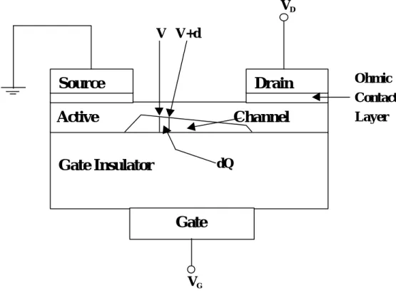
In Fig. 6, we will make the assumptions that electric field of x axis induces
channel and electric field of y axis induces drain current through the
amorphous silicon. As gate voltage is higher than threshole voltage, that is,
mobile carrier is induced in channel, mobile charge, equation of Q1 and gate
voltage, VG is as follows,
QI = -CSiNx(VG – VTH), [eq. 1.]
where channel voltage is 0V. Because potential V is induced by bias
between drain and source in y axis actually, mobile carrier induced in
channel is modified as follows,
QI = -CSiNx(VG – VTH –V), [eq. 2.]
On the other hand, channel current induced by majority carrier is as follows,
ID = WµnQ1Ey, [eq. 3]
where W is channel width. Combining equations Ey = -dV/dy, eq. 2, and eq.
3, we find that
IDdy=Wµn CSiNx(VG – VTH –V)dV, [eq. 4]
We can now integrate equation 4 over the length of the channel and from
V=0 to VD. We have
] 2V )V 1 V L[(V
ì W C
ID = SiNx n G − TH D − D2 , [eq. 5]
From equation 5, we can write, for very small values of VD(VD<1V),
D TH G n
SiNx
D (V V )V
L ì W C
I = − , [eq. 6]
In linear region, field-effect mobility, µn of thin-film transistor is obtained
from equstion 6.
Saturation region
When VD becomes larger than the VD(sat) value, the point in the channel
at which the inversion charge is just zero moves toward the source terminal.
In this case, electrons enter the channel at the source, travel through the
channel toward the drain, and then, at the point where the charge goes to
zero, the electrons are injected into the space charge region where they are
swept by the E-field to the drain contact. If we assume that the change in channel length ∆L is small compared to the original length L, then the drain
current will be a constant for VD>VD(sat). The region of the ID versus VD
characteristic is referred to as the saturation region. In the saturation region,
we will have
2 TH G n SiNx
D (V V )
2L W ì
I =C − , [eq. 7]
The characteristics of thin-film transistor are dependant on a-Si, interface
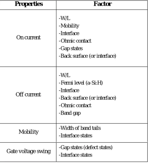
between a-Si and insulator, and contact of a-Si and metal. Table 1 shows
factors affected on characteristics of TFT.
Subthreshole Slope
The subthreshole slope is obtained from S = (d(log Id)/dVg)-1.
Fig. 6. Cross-section of a-Si:H TFT
Gate Insulator
Source Drain
Gate
Active Channel
V V+d
dQ
VD
VG
Ohmic Contact Layer
Properties Factor
On current
-W/L -Mobility -Interface -Ohmic contact -Gap states
-Back surface (or interface)
Off current
-W/L
-Fermi level (a-Si:H) -Interface
-Back surface (or interface) -Ohmic contact
-Band gap
Mobility -Width of band tails -Interface states
Gate voltage swing -Gap states (defect states) -Interface states
Table 1. The properties and factors of thin-film transistor.
2.1.14. Thin Film Transistor Design
There are two of a-Si TFTs : staggered-type and inverse-staggered-type.
For the inverse-staggered-type, the ohmic layer (n+ a-Si) in the channel
region can be etched either directly (etch-back method) or by forming a
protective film on the a-Si thin film (etch-stopper method). Each type has
its own set of advantage and disadvantages. The inverse-staggered structure
offers a relatively simple fabrication process and an electron mobility that is
~30% larger than that of the staggered type. These advantages result that
the bottom-gate TFT structure becomes most widely used in TFT-LCD
although it’s upside-down structure.
Because a-Si has photoelectric characteristics the a-Si TFT must be
shielded from incident light and a-Si layer must be as thin as possible to
minimize the generation of photo-current that can cause malfunction of the
TFT operation. In the staggered-type structure, a light shield layer must be
formed first at the region of TFT channel. The formation of this light shield
layer can be an extra process step. By contrast, in the inverse-staggered-
type TFT’s, a gate electrode is formed first at the TFT channel region and it
also works as a light shield layer. The sizes of the electrodes with W/L ratio
and the overlap between the gate electrode and source-drain electrodes are
the parameters that determine the characteristics of the TFT. The parasitic
capacitances due to overlap of electrodes are not avoidable in staggered
TFT structures but these effects must be minimize to improve the
performance of LCD. In practical operation of the TFT panel, the gate
voltage is set either at 20V for switch-on, ar at –5V for switch-off. Under
these operation conditions the a-Si TFT exhibits as s good switching device
whose on/off current ratio is larger than 106.
The performance of the TFT also depends on the fabrication process
parameters, such as electron mobility and thickness of the gate insulators.
To increase the on-current of TFT, the W/L must be increased if the process
parameters are fixed. However, the larger W/L cause the lower aperture
ratio.
2.2. Cu-alloy process
The addition of an alloying agent to pure Cu may be needed to establish
the most reliable interconnections, with improved electromigration
resistance, corrosion resistance, adhesion, and stability against hillock and
void formation[59]. Many alloying elements have low solubility in Cu,
enabling the resistivity to be lowered by appropriate heat treatments that
precipitate the alloying element either as a second elemental phase within
the Cu matrix, or as a Cu-compound precipitate. Doping with Al or Mg can
be exceedingly effective in passivating copper surfaces[23]. There are many
other methods that have been explored for surface passivation, including
doping with refractory metals[60-64], formation of surface silicides[65, 66],
and treatment with organic inhibitors[67]. These are not discussed here,
except to say that the general approach advocated in the present paper is
similar to the method advocated by the groups at Cornell and Arizona[60,
61], except that they have concentrated on doping with refractory metals
and have formed surface nitrides instead of oxides. Their approach has been
recently reviewed[60]. There are two important general advantages in using
Al or Mg over refractory metals in order to passivate copper[27, 28]. The
first is the lower annealing temperatures required to transport Al or Mg
compared with those needed for most refractory metals. This may become
very important if polymers are introduced as dielectrics. The second is that
the presence of residual Mg, and to a lesser degree Al, dissolved in the bulk
of the copper conductor results in a much smaller increase in resistivity than
is the case for most refractory metals. For example, the increase in
resistivity per dopant atom added copper is two orders of magnitude smaller
for Mg than it is for Ti. Another advantage is that Al is a very familiar
ingredient in modern microelectronics and, hence, use of Al as a dopant
would require less investment in new manufacturing equipment and is less
likely to present some unanticipated problem in the future[23].
2.2.1. Doping copper by ion implantation
It has been known for half a century that copper oxide grows primarily
by the transport of Cu+ from the metal, through the growing oxide, to the
surface where it is oxidized[68]. This growth mechanism is illustrated
schematically in Fig. 7. Futher, the Cu+ ion transport is believed to occur
via ions hopping between vacancies in the Cu2O[68]. One approach toward
Fig. 7. A schematic representation of how copper oxidizes in air. The oxide grows by Cu+ ions being transported through the growing oxide combining with oxygen at the surface. Blocking Cu+ ion transport through the oxide is one method to control oxidation.
Cu
2O
O
2Cu
+O
2Oxide Metal
altering the oxidation rate of copper is to control the concentration of
vacancies available to this transport mechanism. Because the concentration
of these vacancies is small, there is the opportunity to control the oxidation
rate of copper with the addition of only a very small concentration of
dopant in the metal (more accurately, in the oxide). Hence, this approach
suggests that it should be possible to reduce the oxidation rate of the metal,
while not introducing enough foreign atoms to significantly change the
good conductivity or other desirable properties of the pure metal[23]. The
above simple description of a method for controlling oxidation rate seems
to be confirmed by experimental studies of copper doped by ion
implantation[69]. Further studies confirm that the defects necessarily
introduced by the ion- implatation process can be thermally annealed away,
thus producing an oxidation-resistant film with the conductivity of pure
copper[24].
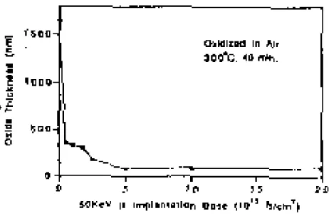
A number of elements can be used to dope copper to reduce the oxidation
rate[24, 69, 70, 71]. Fig. 8 shows some data obtained for B implants
illustrating this general approach[24]. It seems likely that ion implantation
is a feasible method by which to pasivate the exposed surface of copper
metallization lines in microelectronics. The implant doses are modest,
implant ions that are familiar to the electronics industry(such as B) can by
used, the implant modifies only the near surface of the metal and side-
effects of such implants(both on the conductor itself and on other parts of
the device) should be minimal, and the passivation effect is large. However,
it is not clear that in terms of economy of manufacturing, ion implantation
is the most satisfactory method for copper passivation. As indicated below,
other methods provide even more complete passivation and, in addition,
provide substantial improvements in other material properties of copper.
Hence, these approaches may turn out to be even more attractive to
manufacturing than ion implantation. Whether ion implantation will be
comopetitive can be determined only after coomparisos with other
approaches in studies which integrate all the necessary manufacturing steps
[23].
Fig. 8. The thickness of oxide that develors on the surface of copper as a result of heating in air at 300℃ for 40min is plotted vs. the dose of 50keV B implanted into the copper. Notice that even very small implant doses dramatically decrease the oxidation rate of the metal. Data from Ref. [24].
2.2.2. Doping copper during deposition
The evidence from ion implantation is that the addition of small
concentrations of various elements can dramatically reduce the oxidation
rate of copper through the vacancy-blocking mechanism outlined above. As
a further confirmation of this model, experiments were introduced into the
copper during deposition. Observation of the same effects as those seen in
the ion-implanted samples would rule out any specific ion-implantation
effects(such as surface carbon deposition during implantation or structural
alteration of the sample) from contribution to the oxidation resistance. A
passivation by the formation of a barrier layer of metal oxide is a common
mechanism for the passivation of metals. It is the mechanism responsible
for the passivation of Al, which is chemically a very reactive metal. And it
is the fact that copper is not an effective barrier layer that leads to the poor
oxidation resistance of pure copper. The fact that this inert surface oxide is
formed as a result of a reaction between the dopant metal and impurities in
the annealing ambient suggests that optimizing this process will require
more careful study of how this oxide is formed. This is discussed in more
detail below. It is also interesting to note that magnesium which does not
always form a self- passivating oxide on the surface of Mg metal, does form
a good barrier oxide when grown on copper. This general mechanism for
formation of a barrier layer of oxide on the surface of copper is
schematically illustrated in Fig. 9. This figure is drawn to suggest that this
process may lead to much more than just passivation of the exposed surface
of copper but it may lead to what the Arizona group has called encapsulated
copper[60]. The data with which to draw such a conclusion is far from
complete, but in addition to the data outlined above concerning the exposed
surface of the metal, there are indications that the dopant metals are also
being oxidized at the interface with the SiO2 substrate. This reaction leads
to much improved adhesion of the metal to the substrate and possibly
forming a barrier oxide at that interface as well at the surface[27, 28]. One
potential complication with Mg is that unlike Al, at a high enough
temperature, Mg reacts with SiO2 to produce free Si[72]. This may present
a limitation to the use of this Mg as a dopant, unless the extent of this
reaction can be limited, possibly by formation of a self-limiting barrier
Fig. 9. A schemetic representation of what happens during the annealing of co-deposited alloy films. The alloying element (dopant) diffuses to the surface of the metal where it forms a surface oxide layer. If this surface oxide is continuous and impervious, it forms an effective barrier to further oxidation.
Substrate
Substrate Cu-alloy
anneal
Cu in Metal
oxide case
oxide(as occurs with Al), or by limiting the amount of Mg available at the
SiO2 interface. More work on these reactions is necessary. Because of the
formation of such effective barrier oxides, it does not seem possible to
observe the vacancy-blocking mechanism which is dominant in the ion-
implanted samples. The barrier oxide prevents oxidation so effectively that
the vacancy-blocking mechanism is not needed to reduce the oxidation. It is
possible that the ease with which apparently pin-hole free barriers are
formed is partly because of the vacancy-blocking mechanism. At any pin-
hole, the vacancy-blocking mechanism may be sufficiently effective to stop
observable oxidation through small holes.
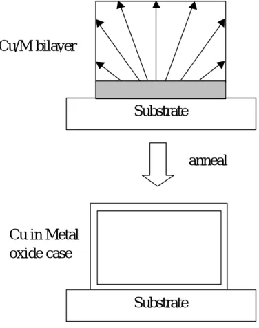
2.2.3. Diffusion doping of copper thin films
Fig. 10 shows a schematic representation of diffusion doping. The basic
idea is to deposit a bilayer of Cu/M/SiO2 where M=Al or Mg, and to anneal
the bilayer. The annealing is intended to first dissolves some of the dopant
metal into the copper, and then to transport it to the surface where it is
oxidezed, as in the alloy case discussed above. A-priori, based on the
results of doping by co-deposition outlined above, it would seem that this
procedure should work, assuming there is sufficient solubility of the dopant
metal in copper and assuming there is no significant competing reaction
between the dopant and the substrate. Both these conditions seem to be
satisfied for Al and Mg, unless the annealing temperature is high enough
that the Mg begins to reduce the SiO2 substrate in comopetition with
dissolution into the copper. However, it might be anticipated that the
annealing process in the bilayer case may be more intricate than in the alloy
case because it will be necessary to dissolve the dopant metal, transport it to
the surface, and then to provide just the right amount of oxygen at that
surface. Too much oxygen before the Al or Mg are prestnt at the surface
will result in oxidation of the copper rather than the formation of the oide
barrier and too little oxygen will not provide the oxygen needed to fully
form the barrier layer[23].
Fig. 10. A schemetic representation of what happens during the annealing of Cu/M/SiO2 bilayer samples. The bilayer metal, M, dissolves into the copper and is then transported to the metal surface where it oxidizes.
Substrate
Substrate Cu/M bilayer
anneal
Cu in Metal
oxide case
3. Experimental
A 1000 Å SiO2 film was formed on a (100) Si wafer by thermal oxidation.
Cu(Mg) alloy films were deposited on the SiO2 by DC magnetron
sputtering from a Cu(4.5 at.% Mg) target which had a purity level of
99.99 %. The sputtering conditions were as follows; the base pressure in the
deposition chamber was 8x10⁻⁷ torr; the Ar pressure was 2 mTorr; the
sputtering power was 180 W; and the substrate temperature was ambient
temperature. Different Cu(Mg) alloy film compositions such as
Cu(4.5at%Mg), Cu(2.3at%Mg), and Cu(1.0at%Mg) were obtained by
controlling the number of Cu chips placed on the target. Different Cu(Mg)
alloy film thickness such as 1000Å, 2000Å and 3000Å were obtained by
controlling the sputtering time. As deposited Cu(4.5Mg)/SiO2/Si multilayer
samples were annealed for 30 minutes in various ambients at O2 pressure
ranging from vacuum to 100mTorr with different film thickness. After
annealing, the resistance as a function of various O2 pressure ambient was
measured by the four point probe method.
To investigate any surface reactions that might occur during PECVD of
SiNx, the pre-annealed multilayer samples were exposed for 10 minutes to
the high density plasma of a SiH4, He and NH3 gas mixture at 400 mTorr
with a substrate temperature of 270 °C. The pre-annealed Cu(Mg) films
were also exposed for 5 minutes to the high density plasma of CF4 at 180
mTorr with a substrate temperature of 120 °C in order to investigate any
surface reactions that might occur during dry etching of the SiNx.
To improve the adhesion strength, 1737 Corning glass was treated by O2
plasma in 100 mTorr at 300℃. Cu-alloy films deposited on the O2 plasma
treated glass were annealed in vacuum at 300℃. Adhesion of Cu-alloy
films to glass substrate was measured by scratch test.
An inverted staggered a-Si:H TFT was fabricated. First, a Cu(Mg) alloy
metal was deposited on glass substrate by sputtering and patterned for gates.
Then, such substrates were annealed at a temperature of 350℃ for 30min
with oxygen ambient. Silicon nitride, undoped a-Si:H, and heavily doped a-
Si:H(n+a-Si:H) films were deposited in a PECVD reactor at 270℃ without
breaking the vacuum. The thicknesses of SiNx, a-Si:H, and n+a-Si:H layers
were 300, 150, 35 nm, respectively. Then 20nm thick Ni layer on the n+a-
Si:H was deposited by RF magnetron sputtering and then source/drain
contacts were defined by using photolithography. The ratio of channel
width to length of the TFT was 78㎛/14㎛. The variation of resistance as a
function of annealing temperature was measured by a four point probe
method. Thickness of Cu-alloy films was estimated by Surface profilometer
and FESEM(Field Emission Scanning Electron Microscopy). X-ray
diffraction (XRD) was employed to identify phases in the Cu alloy films.
The degree of diffusion and interface reaction taking place in the multilayer
systems was evaluated by Auger electron spectroscopy (AES)
compositional depth profiles. Cross-sectional transmission electron
microscopy (XTEM) was used to obtain phase identification of the film as
well as its thickness.
4. Results
4.1. Resistivity
The dependence of resistivity on annealing temperature, thickness, and
Mg contents of the Cu-alloy film is shown in Fig. 11. Three different
Cu(Mg) alloy films containing 4.5, 2.3, and 1.0 at. % Mg were prepared
with various thickness of 1000Å, 2000Å and 3000Å. As Cu(4.5at%Mg)
films are subjected to the vacuum annealing process at various temperatures from 200℃ to 600℃ for 30 min, the resistivity decreased from 12.6µΩ-
cm to 5.5µΩ-cm(Fig. 11(c)). Upon annealing, resistivity of the Cu(Mg)
alloy films with the Mg content of 2.3 and 1.0 atom % also decreased.
Lowest resistivity of Cu-alloy films has been obtained by annealing the
Cu(1.0at%Mg).
Fig. 12 shows the resistivity variation of Cu(4.5at%Mg)/SiO2/Si
multilayer annealed for 30 minutes in O2 pressure of 10mTorr at various
temperatures from 200℃ to 700℃. The resistivity of Cu(Mg) films with
thickness of 1000 Å, 2000 Å and 3000 Å continue to decrease upon annealing
up to 600℃ and then increased abruptly at 700℃. As the thickness of
Fig. 11. Resistivity variation of (a)Cu(1.0at%Mg), (b)Cu(2.3at%Mg), and (c)Cu(4.5at%Mg) films with various thickness annealed in vacuum for 30min at various annealing temperatures.
As-dep 200 300 400 500 600
1.0 1.5 2.0 2.5 3.0 3.5 4.0 4.5 5.0
C u ( 1 . 0 a t % M g ) 2 9 0 0 A C u ( 1 . 0 a t % M g ) 2 0 0 0 A
C u ( 1 . 0 a t % M g ) 1 1 0 0 A
Resistivity(µΩ-cm)
Anneal Temperature(oC)
As-dep 200 300 400 500 600
1.5 2.0 2.5 3.0 3.5 4.0 4.5 5.0 5.5 6.0
C u ( 2 . 3 a t % M g ) 2 9 0 0 A C u ( 2 . 3 a t % M g ) 2 0 0 0 A C u ( 2 . 3 a t % M g ) 1 1 0 0 A
Resistivity(µΩ-cm)
Anneal Temperature(oC)
As-dep 200 300 400 500 600
2 3 4 5 6 7 8 9 10 11 12 13
C u ( 4 . 5 a t % M g ) 2 9 0 0 A C u ( 4 . 5 a t % M g ) 2 0 0 0 A
C u ( 4 . 5 a t % M g ) 1 1 0 0 A
Resistivity(µΩ-cm)
Anneal Temperature(oC)
(a)
(c)
(b)
Fig. 12. Resistivity variation of Cu(4.5at%Mg) films annealed in O2
pressure of 10mTorr for 30 min at various temperatures.
As-dep 300 400 500 600 700
2.5 5.0 7.5 10.0 12.5
Cu(4.5at%Mg) 3000A
Cu(4.5at%Mg) 2000A Cu(4.5at%Mg) 1000A
Resistivity(µΩ-cm)
Anneal Temp(oC)
Cu(Mg) films increased the resistivity also increased. Compared to vacuum
annealing shown in Fig. 11, the magnitude of reduced resistivity was
prominent especially in the case of 1000Å Cu(4.5at%Mg) film. This
reason can be due to the fast diffusion of Mg into the surface to form a
dense MgO, resulting in the lower content of Mg in the alloy film.
To investigate the passivation capability of MgO layers formed by
annealing 4000Å Cu(Mg) films in vacuum, an additional 10 min annealing at 320°C in an atmospheric ambient was carried out. Fig. 13 shows the
results on the passivation capability of the self-encapsulated Cu alloy films.
Fail and pass in the figure mean that oxidation and nonoxidation occurred
on the vacuum-annealed Cu(Mg)/SiO2/Si multiplayer system during the
atmospheric annealing, respectively. Fail and pass tests were determined by
resistivity measurment and SEM. It can be clearly seen that MgO layers
obtained from Cu(2.3at%Mg) and Cu(4.5at%Mg) films effectively
passivated Cu against the environmental oxidation while maintaining low
resistivity.
Fig. 13. Effects of annealing temperature, Mg contents, and thickness on
the passivation failure.
X X
3000
2000
1000
2.3 4.5 1.0
Thickness(A)
Mg Content(at%)
X
2.3 4.5 1.0
3000
2000
1000
Thickness(A)
Mg Content(at%)
3000
2000
1000
4.5 1.0 2.3
Thickness(A)
Mg Content(at%)
3000
2000
1000
2.3 4.5 1.0
Thickness(A)
Mg Content(at%)
300℃
600℃
500℃
400℃
To investigate the effect of O2 ambient annealing on the resistivity, as-
deposited Cu(4.5 at.%Mg)/SiO2/Si multilayer samples with various
thickness were annealed for 30 minutes in a various oxygen pressure ambient at 400 °C . Results are shown in Fig. 14. The magnitude of reduced
resistivity was significant especially in the case of 1000Å Cu(4.5at%Mg)
film upon annealing in 8 mTorr O2 ambient compared to vacuum annealing.
This reason was found to be due to extensive grain growth of Cu, which
was confirmed by TEM as shown in Fig. 15. Extensive grain growth in the
case of 1000Å Cu(Mg) film upon annealing can be seen in Fig. 15. These
results suggest that the mobility of Mg can be accelerated by the reaction of
8 mTorr O2, providing more energy released to affect the microstructural
change. Careful inspection of the AES depth profiles of this multilayer
sample (Fig. 16) showed that a small amount of C had been transported to
the 1000Å Cu(Mg) alloy film after annealing in vacuum. However, 1000
Å Cu(4.5Mg) annealed in O2 8mTorr ambient revealed improved
passivation capacity since significant amount of Mg exists on the Cu
surface with very small a mount of C compared to the film annealed in
vacuum. On the other hand, no significant effects of annealing ambient on
the microstructural change of 2000Å and 3000Å Cu(Mg) films have been
observed. From these results, it can be known that annealing in O2 ambient
enhances Mg diffusion to the Cu surface by the formation of denser MgO
layer. It thus appears that the effect of O2 annealing on the resistivity is
more significant in the case of thinner films by affecting the easy grain
growth.
Fig. 17. shows XRD patterns of the Cu(4.5 at.% Mg)/SiO2/Si multilayer
system which was annealed at 400 °C for 30 minutes in various O2
pressures. With an O2 pressure of 8mTorr and vacuum in 1000 Å thin film,
the surface MgO layer has been effectively formed, as confirmed by the
absence of Cu oxide peaks. From these results, it appears that a self-
aligned MgO layer forms effectively regardless of thickness and in low O2
pressure ambient.
Fig. 14.Effects of annealing temperature, Mg contents, and thickness on the
passivation properties.
As-dep Vacuum 8 50 100
2.5 5.0 7.5 10.0
12.5 Anneal Time : 30min
Cu(4.5at%Mg) 2000A
Cu(4.5at%Mg) 3000A Cu(4.5at%Mg) 1000A
Resistivity( µΩ -cm)
Pressure(mTorr)
Fig. 15. TEM images of Cu(4.5 at.%Mg)/SiO2/Si mutilayer samples with a
thickness of (a) 1000 Å, (b)2000 Å, and (c)3000 Å annealed in
vacuum and (d)1000 Å, (e)2000 Å, and (f)3000 Å annealed in 8mTorr
of O2.