- 1140 -
A Study on the Small Signal Modeling of Smart Power IC
Hai Xu*, Hee-Jun Kim*, and Kyu-Min Cho**
* School of Electrical and Computer Eng., Hanyang University
** Dept. of Information and Communications, Yuhan College
Abstract - A method of modeling the Smart Power IC is presented in this paper, which is based on the IC's typical operation characteristics and small signal frequency response data. Using the least square identification, the IC's dynamic mathematical model, which is expressed as transfer function, can be synthesized from the experimentally obtained gain and phase data. The practicability and effectiveness of the method are verified by means of experiments.
1. Introduction
A major trend in today's Power Integrated Circuit (IC) development is to create Smart Power ICs [1]. Considering the large application potential of Power ICs [2], an enormous growth is expected in high-density consumer applications of monolithic Smart Power ICs' solutions. With more needs of flexibility and model predictive control to Smart Power ICs, there are more demands for the correct parameters and dynamic response of a single Smart Power IC. Therefore, it is important to identify the IC's dynamic mathematic model.
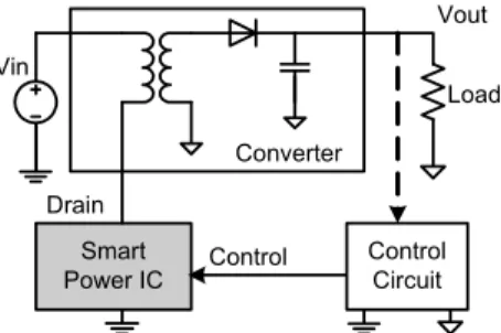
A typical switch-mode power supply (SMPS) with a Smart Power IC is shown in Fig. 1. The switching converter can be a Flyback or a Forward converter. The control circuit can be a feedback or a forward control circuit. The three most popular pins of the Smart Power IC shown in Fig.1 are Drain pin, Control pin and Source pin (or power ground pin). The IC, as a pulse-width modulation (PWM) controller, converts a voltage or a current at the Control input to a duty cycle at the Drain output of the power MOSFET.
A main problem of obtaining the Smart Power IC's transfer function in a direct way is due to the high voltage of the Drain output. Even though the analog signal through Control input is a continuous function of time, there can be only one discrete value of the duty cycle during every switching period, and the voltage amplitude of Drain also varies greatly.
So it is difficult to measure the duty cycle directly.
The purpose of this paper is to obtain the Smart Power IC's frequency response indirectly and to model its transfer function via a set of small signal experimental frequency response data.
Smart Power IC Drain
Control Control Circuit
Load Vin
Converter
Vout
Fig. 1. Simplified SMPS circuit diagram with a Smart Power IC.
2. Small Signal Modeling
To analyze the SMPS frequency response, let us perturb and linearize the average signals about the quiescent operation points [3]. The small signal block diagram shown in Fig.2 contains: ′ ′ -Smart Power IC transfer function, ′ ′ -converter control-to-output
transfer function, -converter line-to-output transfer function, -converter output impedance. The transfer function from the Control input to the power supply output in the open-loop converter becomes:
′′ . (1)
Smart IC Drain
Control
Control Circuit
Load Converter
ˆout ˆ v
ˆ
( ,v iin load) G Zvg, out
ˆd′ vˆCtrl
( )
Gd c′ s
⊕ Gvd′
Fig. 2. Small signal block diagram of the SMPS with a Smart Power IC.
Then the Smart Power IC is replaced by a traditional PWM and power MOSFET circuit at the same quiescent operation points, as shown in Fig.3, and the corresponding small signal block diagram is shown in Fig.4, containing -PWM IC transfer function which is known beforehand, ′ ′ -converter control-to-output transfer function, -converter line-to-output transfer function,
-converter output impedance. Considering about
′ for the power MOSFET, the transfer function from the Control input to the power supply output in the open-loop converter becomes:
′ . (2)
As the same converter is operated at the same quiescent operation points, thus
′ ′ . (3)
With the known and the measured and , substitution of Eq.(2) and Eq.(3) into Eq.(1) leads to the following expression for the measured Smart Power IC transfer function:
′
. (4) The experimental data will be suffered from many kinds of noise.
Based on Central Limit Theorem, the sum of all the independent and identically-distributed random noise will tend to be approximately normally distributed. So the experimental frequency response data are 2007년도 대한전기학회 하계학술대회 논문집 2007. 7. 18 - 20
- 1141 -
then processed by using Monte Carlo method. And the polynomial coefficients for this Single-Input Single-Output (SISO) transfer function are identified with the least square technique [4].
Vin
PWM MOSFET
Circuit Drain
Control Control Circuit
Load
Converter
Vout
Fig. 3. Simplified SMPS circuit diagram with a traditional PWM and power MOSFET circuit replacing the Smart Power IC for the same switching converter.
Drain
Control
Control Circuit
Load ˆ*out
v
ˆd′*
ˆCtrl*
( )
v*
Gdc s ˆd*
*
Gvd′
⊕ Converter
* , * vg out
G Z
* ˆ*
( ,v iˆin load)
MOSFET
Fig. 4. Small signal block diagram corresponding to SMPS with the traditional PWM circuit.
Fig. 5. Experiment data of the Smart Power IC's frequency response and the traditional PWM circuit's frequency response.
3. Experimental Results
To verify the above principle, a 200V/12V, 2A, 100 kHz Flyback power supply is used as an experimental prototype. A device TOP224 [5]
is used as the Smart Power IC in Fig.1, and a circuit including a PWM-control IC TL494 and a MOSFET FQP6N60 works as the traditional PWM and power MOSFET circuit in Fig.3.
The frequency responses, in Eq.(1) and in Eq.(3), are measured 50 times respectively. Then we get the average results of the measured frequency responses, as shown in Fig.5. The line curve in Fig.5 indicates , the transfer function from the Control input of the Smart Power IC TOP224 to the power supply output, and the dashed line curve indicates , the transfer function from the Control input of the PWM-control IC TL494 to the power supply output.
Based on the well-known PWM-control IC TL494's transfer function
, we can get the Smart Power IC's frequency response ′
through Eq.(4), with the measured and . Using the least square technique [4], we can identify the Smart Power IC TOP224's model′, as Eq.(5). It shows that the measured TOP224's DC gain is 153 (43.7dB) and the dominant pole in the transfer function is 7.37 kHz.
′
≈
∙
. (5)
According to TOP224 data sheet [5], its DC gain for reference is 160 (44.0dB) and its transfer function pole is 7 kHz. The comparison between the experimental results and the reference characters has been made in Fig.6, which shows the identified model's transfer function curves (line) are well accorded with the reference model's curves (dashed line). When the signal frequency was higher than 10 kHz, there was some difference between the experimental phase-frequency response (dot line) from the identified model transfer function (line) and the reference transfer function (dashed line). This was because the 100 kHz switching frequency caused much noise to the measured phase-frequency response data [3].
Fig. 6. Comparison of the frequency responses of experimental data, identified model and reference model.
4. Conclusion
This paper demonstrated an indirect modeling method to obtain a Smart Power IC's transfer function via experimental frequency response data. The whole process is as follow: first measuring the control-to-output transfer functions of the power supply with the Smart Power IC and those with the PWM and MOSFET circuit respectively, then calculating the Smart Power IC's frequency responses, and at last identifying the IC's model. The experimental results were presented to show that the small signal modeling method to identify the Smart Power IC dynamic mathematic model is feasible. Although the results of the given case were shown for one simple first order device, it does not seem to have any restriction to other higher order ones.
[Reference]
[1] Gene Heftman, "PWM: From a single chip to a giant industry", Power Electronics Technology Mag., Oct. 2005, pp.48, 50-53.
[2] B. J. Baliga, "An Overview of Smart Power Technology", IEEE Trans. on Electronic Devices, Vol. 38, No.7, July 1991, pp.1568-1575.
[3] R. W. Erickson and D. Maksimovic, Fundamentals of Power Electronics, 2nd ed.
Norwell, Ma: Kluwer, 2001.
[4] L. Ljung, System Identification-Theory for the User, 2nd ed. Upper Saddle River, N.J., : Prentice Hall PTR, 1999.
[5] Power Integrations INC, TOP221-227 TOPSwitch-II Family data sheet [Online]. Website: www.powerint.com/PDFFiles/top221-227.pdf